

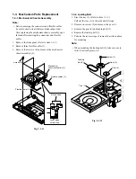


2-6. When Replaced ROM ICs or Upgraded Firmware
1. When replaced the following ROM ICs, it is necessary
to write the data into the new ICs.
1) IC606 (firmware)
2) IC601 (Setup default data and other information)
2. When the firmware is upgraded, rewriting the new
firmware into IC606 may be requested for servicing.
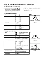
3. Connect a computer to the main PC board of the DVD
video player with using DATA UPDATE KIT (P/No.
79080074). (Fig. 3-2-6)
4. Writing operation
Refer to the instruction attached to the data floppy
disc.
Fig. 3-2-6
Note:
• The firmware and setup data floppy discs are not available as service parts.
For more information, consult TOSHIBA service office in your area.
CN601
DATA UPDATE KIT
(RS232C Interface/cable)
RS-232C
cable
Computer
(MS-DOS/PC-DOS)
Содержание SD-2050
Страница 1: ...DVD VIDEO PLAYER SERVICE MANUAL May 2000 s FILE NO 810 200005 SD 2050 DIGITAL VIDEO ...
Страница 5: ...SECTION 1 GENERAL DESCRIPTIONS SECTION 1 GENERAL DESCRIPTIONS 1 OPERATING INSTRUCTIONS ...
Страница 51: ...47 Others Memo ...
Страница 80: ...4 2 Power Supply Block Diagram Fig 3 4 2 ...
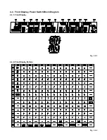
Страница 82: ...Fig 3 4 5 4 3 3 Front Display Power Switch Block Diagram ...
Страница 84: ...Fig 3 4 7 4 4 2 Logical System Block Diagram ...
Страница 85: ...4 5 Output Block Diagram Fig 3 4 8 ...
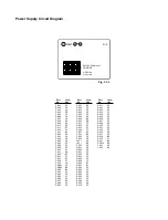
Страница 86: ...10 1 3 4 A B C D E G 2 5 6 7 8 9 F Fig 3 5 1 5 CIRCUIT DIAGRAMS 5 1 Power Supply Circuit Diagram ...
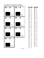
Страница 88: ...10 1 3 4 A B C D E G 2 5 6 7 8 9 F Fig 3 5 3 5 2 Front Display Power Switch Circuit Diagram ...
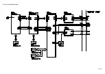
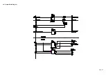
Страница 95: ...Fig 3 5 5 5 3 2 Main Circuit Diagram ...
Страница 96: ...5 3 2 Main Circuit Diagram ...
Страница 97: ......
Страница 98: ......
Страница 99: ......
Страница 100: ......
Страница 101: ......
Страница 102: ......
Страница 103: ...Fig 3 5 5 ...
Страница 105: ...Fig 3 5 6 10 1 3 4 A B C D E G 2 5 6 7 8 9 F 11 H 5 4 Output Circuit Diagram ...
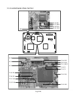
Страница 115: ...10 1 3 4 A B C D E G 2 5 6 7 8 9 F Fig 3 6 6 EU01 Main PC Board Top pattern character symbol ...
Страница 116: ...10 1 3 4 A B C D E G 2 5 6 7 8 9 F Fig 3 6 7 EU01 Main PC Board Bottom pattern character symbol ...
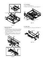
Страница 120: ...4 EXPLODED VIEWS 4 1 Packing Assembly Fig 4 4 1 ZF01 ZF27 ZF17 ZF10 ZF11 ZF23 ZF30 ZK04 ZK01 ZK03 ZK02 ...
Страница 125: ......


