


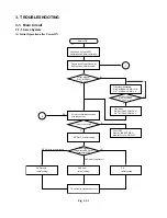


Pickup (P.U.) transmission initial
operation does not occur.
The pickup transmission initial operation is carried out to
determine the initial position by transmitting the pickup to the
innermost position once (start-limit switch (pin 4 of CN503)
develops "L".) and to the external direction at low speed
(start-limit switch develops "H", turning off the switch.).
1
Does pulse of
1.65V 1.65V develop at
pin 162 of IC401?
Check BUS between IC401
and IC604 and oscillation.
Check feed gear.
N
Y
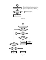
2-1
"No disc" misjudgement display of
disc presence.
Does lens move with
UP/DOWN full stroke in
focus direction?
Is laser current normal?
Check IC401.
Does search signal
output at both edges of focus coil?
(Pins 10 to 13 of CN501)
Does focus search
voltage of 1.65V 0.4V develop
at pin 1 of IC503 (E546)?
Check pickup head
and wiring.
Does RFSB signal
develop more than 0.3V?
Check IC502.
Lens cleaning.
Replace pickup head.
Check peripheral
circuit of IC604.
Check IC502.
Y
Y
Y
Y
3
N
N
N
Y
N
N
Fig. 1-3-2
Fig. 1-3-3
Содержание SD-2050
Страница 1: ...DVD VIDEO PLAYER SERVICE MANUAL May 2000 s FILE NO 810 200005 SD 2050 DIGITAL VIDEO ...
Страница 5: ...SECTION 1 GENERAL DESCRIPTIONS SECTION 1 GENERAL DESCRIPTIONS 1 OPERATING INSTRUCTIONS ...
Страница 51: ...47 Others Memo ...
Страница 80: ...4 2 Power Supply Block Diagram Fig 3 4 2 ...
Страница 82: ...Fig 3 4 5 4 3 3 Front Display Power Switch Block Diagram ...
Страница 84: ...Fig 3 4 7 4 4 2 Logical System Block Diagram ...
Страница 85: ...4 5 Output Block Diagram Fig 3 4 8 ...
Страница 86: ...10 1 3 4 A B C D E G 2 5 6 7 8 9 F Fig 3 5 1 5 CIRCUIT DIAGRAMS 5 1 Power Supply Circuit Diagram ...
Страница 88: ...10 1 3 4 A B C D E G 2 5 6 7 8 9 F Fig 3 5 3 5 2 Front Display Power Switch Circuit Diagram ...
Страница 95: ...Fig 3 5 5 5 3 2 Main Circuit Diagram ...
Страница 96: ...5 3 2 Main Circuit Diagram ...
Страница 97: ......
Страница 98: ......
Страница 99: ......
Страница 100: ......
Страница 101: ......
Страница 102: ......
Страница 103: ...Fig 3 5 5 ...
Страница 105: ...Fig 3 5 6 10 1 3 4 A B C D E G 2 5 6 7 8 9 F 11 H 5 4 Output Circuit Diagram ...
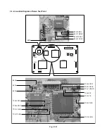
Страница 115: ...10 1 3 4 A B C D E G 2 5 6 7 8 9 F Fig 3 6 6 EU01 Main PC Board Top pattern character symbol ...
Страница 116: ...10 1 3 4 A B C D E G 2 5 6 7 8 9 F Fig 3 6 7 EU01 Main PC Board Bottom pattern character symbol ...
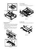
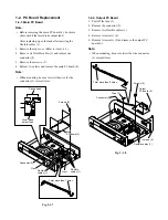
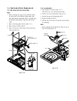
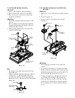
Страница 120: ...4 EXPLODED VIEWS 4 1 Packing Assembly Fig 4 4 1 ZF01 ZF27 ZF17 ZF10 ZF11 ZF23 ZF30 ZK04 ZK01 ZK03 ZK02 ...
Страница 125: ......


