


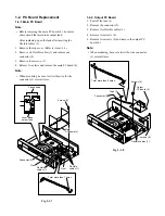


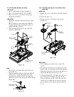


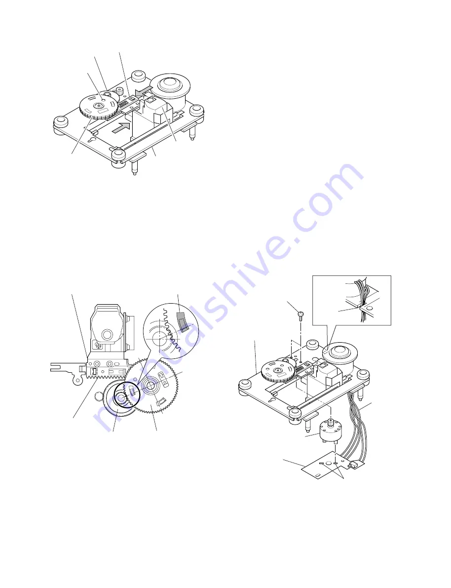
1-3-6. Feed Motor
<Removal>
1. Remove the gear B assembly (1) and the gear A (2).
(Refer to item 1-3-5.)
2. Remove two screws (1) and remove the feed motor (2)
(with the feed motor PC board (3) attached).
(Refer to Fig. 2-1-21.)
3. Desolder the terminals of the feed motor (2) and
remove the feed motor PC board (3).
<Mounting>
1. Tighten the feed motor (2) on the pickup mechanism
assembly with two screws (1).
2. Insert the feed motor PC board (3) with the position-
ing pin on the chassis matched and solder the termi-
nals.
3. Perform the reverse order of the removal.
Note:
• After mounting, put the lead wires through the notch
of the pickup mechanism assembly.
Fig. 2-1-21
Feed motor (2)
Feed motor
PC board (3)
Screws (1)
Pickup mechanism
assembly
Desolder
Lead wires
Notch
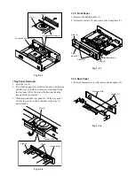
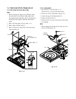
Fig. 2-1-19
Note:
• Mount the gear B assembly (1) and the gear A (2) with
their gear teeth placed more than one tooth at least
inside the shaded portion.
Fig. 2-1-20
Rack gear assembly (4)
Gear A (2)
A
B
Positioning holes
Gear B assembly (1)
Pickup Head (5)
Pickup mechanism
assembly
Gear B assembly (1)
Rack gear assembly (4)
Gear A (2)
Within the position shown
by the shaded porition.
Innermost position
of pickup head
Содержание SD-2050
Страница 1: ...DVD VIDEO PLAYER SERVICE MANUAL May 2000 s FILE NO 810 200005 SD 2050 DIGITAL VIDEO ...
Страница 5: ...SECTION 1 GENERAL DESCRIPTIONS SECTION 1 GENERAL DESCRIPTIONS 1 OPERATING INSTRUCTIONS ...
Страница 51: ...47 Others Memo ...
Страница 80: ...4 2 Power Supply Block Diagram Fig 3 4 2 ...
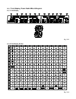
Страница 82: ...Fig 3 4 5 4 3 3 Front Display Power Switch Block Diagram ...
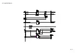
Страница 84: ...Fig 3 4 7 4 4 2 Logical System Block Diagram ...
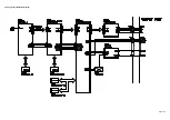
Страница 85: ...4 5 Output Block Diagram Fig 3 4 8 ...
Страница 86: ...10 1 3 4 A B C D E G 2 5 6 7 8 9 F Fig 3 5 1 5 CIRCUIT DIAGRAMS 5 1 Power Supply Circuit Diagram ...
Страница 88: ...10 1 3 4 A B C D E G 2 5 6 7 8 9 F Fig 3 5 3 5 2 Front Display Power Switch Circuit Diagram ...
Страница 95: ...Fig 3 5 5 5 3 2 Main Circuit Diagram ...
Страница 96: ...5 3 2 Main Circuit Diagram ...
Страница 97: ......
Страница 98: ......
Страница 99: ......
Страница 100: ......
Страница 101: ......
Страница 102: ......
Страница 103: ...Fig 3 5 5 ...
Страница 105: ...Fig 3 5 6 10 1 3 4 A B C D E G 2 5 6 7 8 9 F 11 H 5 4 Output Circuit Diagram ...
Страница 115: ...10 1 3 4 A B C D E G 2 5 6 7 8 9 F Fig 3 6 6 EU01 Main PC Board Top pattern character symbol ...
Страница 116: ...10 1 3 4 A B C D E G 2 5 6 7 8 9 F Fig 3 6 7 EU01 Main PC Board Bottom pattern character symbol ...
Страница 120: ...4 EXPLODED VIEWS 4 1 Packing Assembly Fig 4 4 1 ZF01 ZF27 ZF17 ZF10 ZF11 ZF23 ZF30 ZK04 ZK01 ZK03 ZK02 ...
Страница 125: ......


