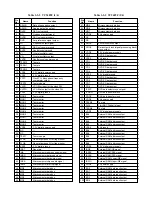
Table 3-5-2 PCM1716E-T
Pin
No.
1
2
3
4
5
6
7
8
9
10
11
12
13
14
15
16
17
18
19
20
21
22
23
24
25
26
27
28
Function
Left and Right Clock Input. This clock is
equal to the sampling rate - l
s
.
(1)
Serial Audio Data Input.
(1)
Bit Clock Input for Serial Audio Data.
(1)
Buffered Output of Oscillator. Equivalent to
System Clock.
Oscillator Input (External Clock Input)
Oscillator Output
Digital Ground
Digital Power +5V
Analog Power +5V
Analog Ground
Rch, Common Pin of Analog Output Amp
No Connection
Rch, Analog Voltage Output of Audio Signal
Analog Ground
Analog Power +5V
Lch, Analog Voltage Output of Audio Signal
No Connection
Lch, Common Pin of Analog Output Amp
Analog Ground
Analog Power +5V
Zero Data Flag
Reset. When this pin is low, the DF and
modulators are held in reset.
(2)
Chip Select/Input Format Selection. When
this pin is low, the Mode Control is
effective.
(3)
Mode Control Select. (H: Software, L:
Hardware)
(2)
Mute Control.
Mode Control, DATA/De-emphasis
Selection 1
(2)
Mode Control, BCK/De-emphasis Selection
2
(2)
Mode Control, WDCK/Input Format
Selection
(2)
Name
LRCIN
DIN
BCKIN
CLKO
XTI
XTO
DGND
V
DD
V
CC
2R
AGND2R
EXTR
NC
V
OUT
R
AGND1
V
CC
1
V
OUT
L
NC
EXTL
AGND2L
V
CC
2L
ZERO
RST
CS/IWO
MODE
MUTE
MD/DM0
MC/DM1
ML/I
2
S
Main ICs Function
Ref. No.
IC601
IC303
IC301
IC401
IC502
IC503
IC906
IC604
IC202
IC606
IC Name
S24C04BFJ-TB
ADV7170
MD36710X
TC9489F
TA1313F
KA3032
PCM1716E
TMP94CS40AF
TC203G08F0103
MBM29F800TB-55
Function
EE-PROM
Video Encorder
AV Decorder
SERVO & Data Processor
RF Signal processing IC
5-CH Motor Driver
DA Converter
Main Micro Processor
Track Buffer
Flash ROM
Detail
Setup default, memorization of specification setting.
Built-in D/A converter. Encodes digital video signal to analog video
signal of NTSC/PAL system.
Decryption, MPEG-2 Decode, Audio Decode, Sub Picture Decode,
OSD.
Performs servo control of DVD or CD, and performs demodulation
and correction of RF signal.
Equalizes of playback RF signal and generates error detection signal
required for each servo operation.
5ch driver for motor driving.
Stereo audio DA converter with a dual PPL built-in.
Performs system control for all circuits.
Rate control and Buffer control.
Memorization for firmware.
Table 3-5-1
Table 3-5-3 PLL1700E-T
Pin
No.
1
2
3
4
5
6
7
8
9
10
11
12
13
14
15
16
17
18
19
20
Function
Latch Enable for Software Mode/Sampling
Rate Selection for Hardware Mode. When
MODE pin is LOW, ML is selected.
(1)
Mode Control Select. When this pin is
HIGH, device is operated in hardware
mode using SR0 (pin 1), FS0 (pin 19), and
FS1 (pin 20). When this pin is LOW, device
is operated in software mode by three-wire
interface using ML (pin 1), MD (pin 19) and
MC (pin 20).
(1)
Digital Power Supply. +5V.
Digital Ground.
27MHz Crystal. When an external 27MHz
clock is applied to XT1 (pin 6), this pin
must be connected to GND.
27MHz Oscillator Input/External 27MHz
input.
Ground for PLL.
Power Supply for PLL +5V.
Reserved. Must be left open.
27MHz Output.
Inverted 27MHz Output.
Fixed 33.8688MHz Clock Output.
768/
s
Clock Output.
256/
s
Clock Output.
Digital Ground for V
DC8
Digital Power Supply for Clock Output
Buffers. +3.3V.
3841
s
Output. This output has been
optimized for the lowest jitter and should
be connected to the audio DAC(s).
Reset. When this pin is LOW, device is
held in reset.
(1)
Serial Data Input for Software Mode/
Sampling Frequency Selection for
Hardware Mode. When MODE pin is LOW.
MD is selected.
(1)
Shift Clock Input for Software Mode/
Sampling Frequency Selection for
Hardware Mode. When MODE pin is LOW.
MC is selected.
(1)
Name
ML/SR0
MODE
V
DD
GND
XT2
XT1
GNDP
V
DDP
RSV
MCKO
MCKO
SCKO1
SCKO4
SCKO2
GNDB
V
DC8
SCKO3
RST
MD/FS0
MC/FS1
Note:(1) Schmitt-trigger input with internal pull-down resistors.
Notes: (1) Pins 1,2,3; Schmitt Trigger input
(2) Pins 22,24,25,26,27,28; Schmitt Trigger input with
pull-up resistor.
(3) Pin 23; Schmitt Trigger input with pull-down
resistor.
Содержание SD-2050
Страница 1: ...DVD VIDEO PLAYER SERVICE MANUAL May 2000 s FILE NO 810 200005 SD 2050 DIGITAL VIDEO ...
Страница 5: ...SECTION 1 GENERAL DESCRIPTIONS SECTION 1 GENERAL DESCRIPTIONS 1 OPERATING INSTRUCTIONS ...
Страница 51: ...47 Others Memo ...
Страница 80: ...4 2 Power Supply Block Diagram Fig 3 4 2 ...
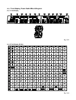
Страница 82: ...Fig 3 4 5 4 3 3 Front Display Power Switch Block Diagram ...
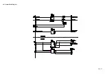
Страница 84: ...Fig 3 4 7 4 4 2 Logical System Block Diagram ...
Страница 85: ...4 5 Output Block Diagram Fig 3 4 8 ...
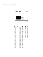
Страница 86: ...10 1 3 4 A B C D E G 2 5 6 7 8 9 F Fig 3 5 1 5 CIRCUIT DIAGRAMS 5 1 Power Supply Circuit Diagram ...
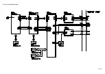
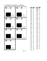
Страница 88: ...10 1 3 4 A B C D E G 2 5 6 7 8 9 F Fig 3 5 3 5 2 Front Display Power Switch Circuit Diagram ...
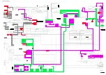
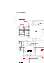
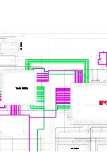
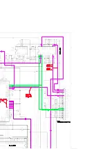
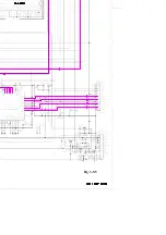
Страница 95: ...Fig 3 5 5 5 3 2 Main Circuit Diagram ...
Страница 96: ...5 3 2 Main Circuit Diagram ...
Страница 97: ......
Страница 98: ......
Страница 99: ......
Страница 100: ......
Страница 101: ......
Страница 102: ......
Страница 103: ...Fig 3 5 5 ...
Страница 105: ...Fig 3 5 6 10 1 3 4 A B C D E G 2 5 6 7 8 9 F 11 H 5 4 Output Circuit Diagram ...
Страница 115: ...10 1 3 4 A B C D E G 2 5 6 7 8 9 F Fig 3 6 6 EU01 Main PC Board Top pattern character symbol ...
Страница 116: ...10 1 3 4 A B C D E G 2 5 6 7 8 9 F Fig 3 6 7 EU01 Main PC Board Bottom pattern character symbol ...
Страница 120: ...4 EXPLODED VIEWS 4 1 Packing Assembly Fig 4 4 1 ZF01 ZF27 ZF17 ZF10 ZF11 ZF23 ZF30 ZK04 ZK01 ZK03 ZK02 ...
Страница 125: ......


