


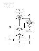


3. TROUBLESHOOTING
3-1. Main Circuit
3-1-1. Servo System
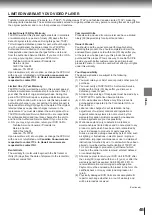
(1) Initial Operation after Power ON
Power ON
Send each LSI hard RST
command and initial command.
Pickup head is positioned at
transmission initial position.
Is tray closed?
Pin 5 of CN502,
TCLS=L
Disc presence/absence and
disc judgement
Is a disc present?
DVD or CD initial setting.
DVD single
Initial setting.
DVD dual
Initial setting.
CD
Initial setting.
To each disc playback process.
DVD single (single-layer)
DVD single
(single-layer)/DVD dual
(dual-layer)/CD?
CD
DVD dual (dual-layer)
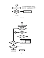
1
Tray close operation
Pin 6 of IC604: LDMP = H/L
Pin 7 of IC604: LDMN = L
Is tray closed?
Pin 5 of CN502:
TCLS = L
Y
N
Tray stops.
Pin 6 of IC604: LDMP = H
Pin 7 of IC604: LDMN = L
Laser OFF
Display: INSERT DISC
Monitor screen: NO DISC
Y
Y
NG
N
N
2
Fig. 1-3-1
Содержание SD-2050
Страница 1: ...DVD VIDEO PLAYER SERVICE MANUAL May 2000 s FILE NO 810 200005 SD 2050 DIGITAL VIDEO ...
Страница 5: ...SECTION 1 GENERAL DESCRIPTIONS SECTION 1 GENERAL DESCRIPTIONS 1 OPERATING INSTRUCTIONS ...
Страница 51: ...47 Others Memo ...
Страница 80: ...4 2 Power Supply Block Diagram Fig 3 4 2 ...
Страница 82: ...Fig 3 4 5 4 3 3 Front Display Power Switch Block Diagram ...
Страница 84: ...Fig 3 4 7 4 4 2 Logical System Block Diagram ...
Страница 85: ...4 5 Output Block Diagram Fig 3 4 8 ...
Страница 86: ...10 1 3 4 A B C D E G 2 5 6 7 8 9 F Fig 3 5 1 5 CIRCUIT DIAGRAMS 5 1 Power Supply Circuit Diagram ...
Страница 88: ...10 1 3 4 A B C D E G 2 5 6 7 8 9 F Fig 3 5 3 5 2 Front Display Power Switch Circuit Diagram ...
Страница 95: ...Fig 3 5 5 5 3 2 Main Circuit Diagram ...
Страница 96: ...5 3 2 Main Circuit Diagram ...
Страница 97: ......
Страница 98: ......
Страница 99: ......
Страница 100: ......
Страница 101: ......
Страница 102: ......
Страница 103: ...Fig 3 5 5 ...
Страница 105: ...Fig 3 5 6 10 1 3 4 A B C D E G 2 5 6 7 8 9 F 11 H 5 4 Output Circuit Diagram ...
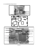
Страница 115: ...10 1 3 4 A B C D E G 2 5 6 7 8 9 F Fig 3 6 6 EU01 Main PC Board Top pattern character symbol ...
Страница 116: ...10 1 3 4 A B C D E G 2 5 6 7 8 9 F Fig 3 6 7 EU01 Main PC Board Bottom pattern character symbol ...
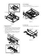
Страница 120: ...4 EXPLODED VIEWS 4 1 Packing Assembly Fig 4 4 1 ZF01 ZF27 ZF17 ZF10 ZF11 ZF23 ZF30 ZK04 ZK01 ZK03 ZK02 ...
Страница 125: ......


