DAC and ADC GUI Configuration File Changes When Using a Xilinx Development Platform
33
SLAU580B – June 2014 – Revised September 2016
Copyright © 2014–2016, Texas Instruments Incorporated
TSW14J10 FMC-USB Interposer Card
4. Connect a micro USB cable between J1 of the ZC706 and a host computer with Vivado loaded.
5. Connect a USB cable between the TSW14J10 and a host computer with HSDC Pro GUI loaded.
6. Connect a USB cable between the DAC38J84 and a host computer with DAC3XJ8X GUI loaded.
Power up the DAC38J84 and ZC706. Program the DAC38J84 per instructions in
.
To program the FPGA, complete the following steps:
1. Due to an issue Vivado has with the file path name, move the file “TSW14J10_ZC706_2vp8.bit”,
located at C:\Program Files(86)\Texas Instruments\High Speed Data Converter Pro\14J10ZC706
Details\Firmware” to C:\.
2. Open Xilinx Vivado design tool.
3. Double click on “Open Hardware Manager”.
4. Click on “Open Target”.
5. Select “Open New Target”. Click on “Next”.
6. Click on “Finish”.
7. Click on “Program device”. Select the device that appears.
8. Navigate to C:\
9. Select “TSW14J10_ZC706_2vp8.bit.
10. Click on “Program device”.
11. A new window will open showing the status of the programming. Once this reached 100%, the FPGA
is programmed and ready to be used with the TSW14J10 to run the HSDC Pro GUI.
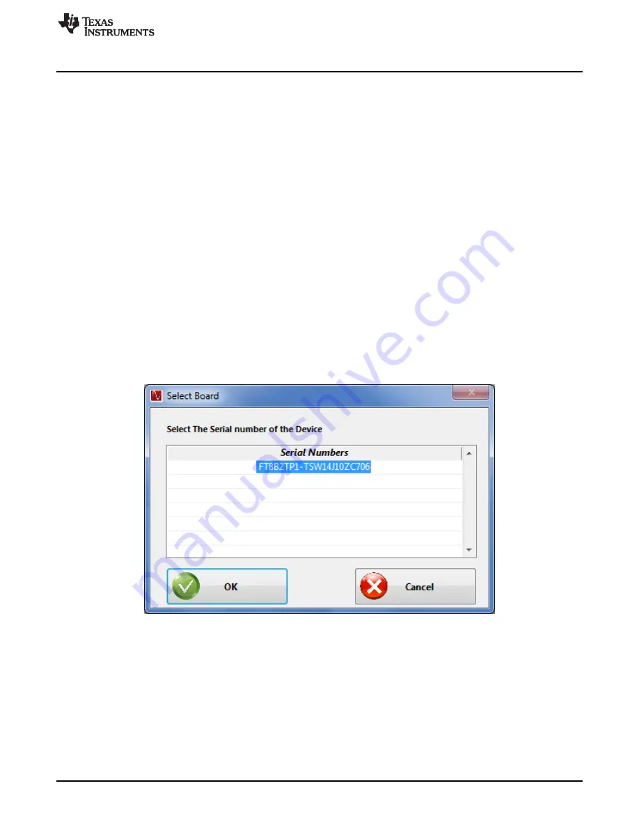
Open HSDC Pro GUI. A new window opens indicating a connection to the ZC706, as shown in
.
Figure 27. Serial Number Selection Window
In the GUI, select the
DAC
tab, then select DAC3XJ84_LMF_442 in the device button. After the firmware
is loaded, enter 368.64M in the
Data Rate (SPS)
window, select 2’s complement in the
DAC Output
window and generate a 10-MHz test tone using the IQ Multitone Generator located in the lower left of the
GUI. Click the
Create Tones
button. The display will appear as shown in


