18
SLOS758G – DECEMBER 2011 – REVISED MARCH 2020
Product Folder Links:
Detailed Description
Copyright © 2011–2020, Texas Instruments Incorporated
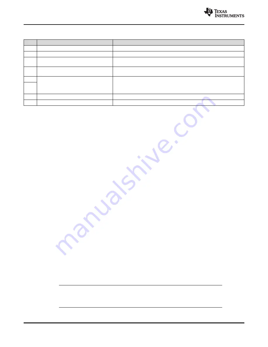
Table 6-4. RX Special Setting Register (0x0A)
BIT
FUNCTION
COMMENTS
B7
Band-pass filter from 110 kHz to 570 kHz
Appropriate for any 212-kHz subcarrier systems like FeliCa
B6
Band-pass filter from 200 kHz to 900 kHz
B5
Band-pass filter from 450 kHz to 1.5 MHz
Appropriate for Manchester-coded 106-kbps 848-kHz subcarrier systems (for
example, used in ISO/IEC 14443 A).
B4
Band-pass filter from 100 kHz to 1.5 MHz
Appropriate for highest bit rate (848 kbps) used in high-bit-rate ISO/IEC 14443 B.
Gain is reduced by 7 dB.
B3
00 = No gain reduction
01 = Gain reduction for 5 dB
10 = Gain reduction for 10 dB
11 = Gain reduction for 15 dB
Sets the RX digital gain reduction (changing the window of the digitizing
comparator).
B2
B1
Reserved
B0
Reserved
6.7
Receiver – Digital Section
The output of the TRF7963A analog receiver block is a digitized subcarrier signal and is the input to the
digital receiver block, which consists of two sections that partly overlap. The digitized subcarrier signal is a
digital representation of the modulation signal on the RF envelope. The two sections of the digital receiver
block are the protocol bit decoder section and the framing logic section.
The protocol bit decoder section converts the subcarrier coded signal into a serial bit stream and a data
clock. The decoder logic is designed for maximum error tolerance. This tolerance lets the decoder section
successfully decode even partly corrupted subcarrier signals that would otherwise be lost due to noise or
interference.
The framing logic section formats the serial bit stream data from the protocol bit decoder stage into data
bytes. During the formatting process, special signals such as the start of frame (SOF), end of frame
(EOF), start of communication, and end of communication are automatically removed. The parity bits and
CRC bytes are also checked and removed. The end result is "clean" or "raw" data that is then sent to the
12-byte FIFO register where it can be read by the external microcontroller system. Providing the data this
way, in conjunction with the timing register settings of the TRF7963A, means the firmware developer must
know about much less of the finer details of the ISO protocols to create a very robust application,
especially in low-cost platforms where code space is at a premium and high performance is still required.
The start of the receive operation (successfully received SOF) sets the IRQ flags in the IRQ Status
register (0x0C). The end of the receive operation is signaled to the external system MCU by setting pin 13
(IRQ) to high. When data is received in the FIFO, an interrupt is sent to the MCU to signal that there is
data to be read from the FIFO. The FIFO Status register (0x1C) should be used to provide the number of
bytes that should be clocked out during the actual FIFO read. Additionally, an interrupt is sent to the MCU
when the received data occupies 75% of the FIFO capacity to signal that the data should be removed
from the FIFO. That interrupt is triggered when the received data packet is longer than 9 bytes.
Any error in the data format, parity, or CRC is detected and notified to the external system by an interrupt
request pulse. The source condition of the interrupt request pulse is available in the IRQ Status register
(0x0C). The main register controlling the digital part of the receiver is the ISO Control register (0x01). By
writing to this register, the user selects the protocol to be used. With each new write in this register, the
default presets are reloaded in all related registers, so no further adjustments in other registers are
needed for proper operation.
NOTE
If additional register setting changes are needed to fine-tune the system, set the ISO Control
register (0x01) before making the additional changes.


