Table 8-13. ADC Electrical Specifications (continued)
PARAMETER
DESCRIPTION
TEST CONDITIONS /
ASSUMPTIONS
MIN
TYP
MAX
UNIT
Input impedance
ADC Pin 57
2.15
kΩ
ADC Pin 58
0.7
ADC Pin 59
2.12
ADC Pin 60
1.17
Number of channels
4
F
sample
Sampling rate of each pin
62.5
KSPS
F_input_max
Maximum input signal frequency
31
kHz
SINAD
Signal-to-noise and distortion
Input frequency DC to 300 Hz
and 1.4 V
pp
sine wave input
55
60
dB
I_active
Active supply current
Average for analog-to-digital
during conversion without
reference current
1.5
mA
I_PD
Power-down supply current for
core supply
Total for analog-to-digital when
not active (this must be the SoC
level test)
1
µA
Absolute offset error
FCLK = 10 MHz
±2
mV
Gain error
±2%
V
ref
ADC reference voltage
1.467
V
8.14.5.7 Camera Parallel Port
The fast camera parallel port interfaces with a variety of external image sensors, stores the image data in a
FIFO, and generates DMA requests. The camera parallel port supports 8 bits.
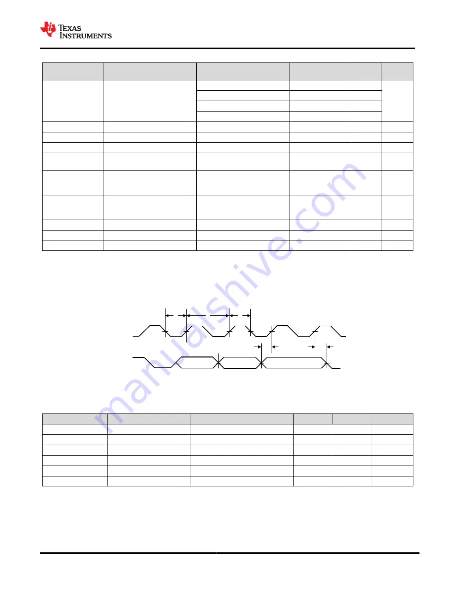
shows the timing diagram for the camera parallel port.
pCLK
pVS, pHS
pDATA
T3
T2
T4
T6
T7
Figure 8-16. Camera Parallel Port Timing Diagram
lists the timing parameters for the camera parallel port.
Table 8-14. Camera Parallel Port Timing Parameters
ITEM
NAME
DESCRIPTION
MIN
MAX
UNIT
pCLK
Clock frequency
2
MHz
T2
T
clk
Clock period
1/pCLK
ns
T3
t
LP
Clock low period
T
clk
/2
ns
T4
t
HT
Clock high period
T
clk
/2
ns
T6
t
IS
RX data setup time
2
ns
T7
t
IH
RX data hold time
2
ns
8.14.5.8 UART
The CC3220MODx and CC3220MODAx modules include two UARTs with the following features:
• Programmable baud-rate generator allowing speeds up to 3 Mbps
• Separate 16-bit × 8-bit TX and RX FIFOs to reduce CPU interrupt service loading
SWRS206E – MARCH 2017 – REVISED MAY 2021
Copyright © 2021 Texas Instruments Incorporated
45
Product Folder Links:


