


xE922-3GR Hardware User Guide
1VV0301272
Rev.0.8 2017-01-05
Reproduction forbidden without written authorization from Telit Communications S.p.A. - All Rights
Reserved.
Page 98 of 112
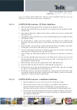
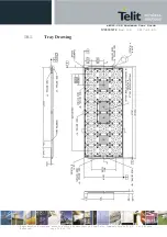
NOTE:
In the customer application, the region under ROUTE INHIBIT (see figure above) must be
clear from signal. The five horseshoe shapes, indicated in the footprint picture above, are solder
resist mask openings in the surrounding GND copper fill. They provide proper GND connection
for built-in RF probes
on Telit’s
production test jig socket. It is not intended to replicate these
horseshoe shapes as well on the
customer’s
module carrier board implementation, the GND
pads surrounding the antenna pads provide solid RF GND.
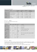
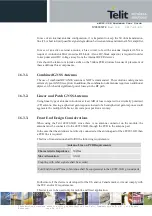
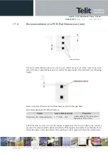
17.4.
Stencil
Stencil’s apertures layout can be the same
as the recommended footprint (1:1). A suggested
thickness of stencil foil is greater than 150 µm.
17.5.
PCB Pad Design
Non solder mask defined (NSMD) type is recommended for the solder pads on the PCB.