


xE922-3GR Hardware User Guide
1VV0301272
Rev.0.8 2017-01-05
Reproduction forbidden without written authorization from Telit Communications S.p.A. - All Rights
Reserved.
Page 41 of 112
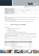
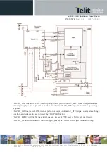
5.
Power supply
5.1.
Input supply
There are 2 input power supplies defined on the xE922-3GR module,
V_BAT, V_BAT_PA.
V_BAT_PA pin supplies transmit RF front end (RFFE) power amplifiers (PA) of the cellular network
(2G/3G) connection feature of the module.
V_BAT pin supplies the remaining module circuitry, distributed via an internal power management unit
(PMU).
Although defined separately, V_BAT and V_BAT_PA can be connected together. The split implementation
allows for separate power consumption characterization of the RFFE as well as optional noise filtering
network to isolate V_BAT from the typical bursty character of V_BAT_PA in 2G mode operation.
NOTE:
In GSM/GPRS mode, RF transmission is not continuous and is packed into bursts at a base
frequency of about 216 Hz with relative current peaks as high as about 2 A. Therefore the power
supply must be designed to withstand these current peaks (from V_BAT_PA input supply pin)
without big voltage drops; this means that both the electrical design (current rating and/or
decoupling buffer capacitors) and the board layout must be designed for this current flow. If
the layout of the PCB is not well designed, a strong noise floor is generated on the ground. This
will reflect on all the audio paths producing an audible annoying noise at 216 Hz; if the voltage
drops during the peaks, current absorption is too high. The device may even shut down as a
consequence of the supply voltage drop.