10 TEGAM WAY • GENEVA, OHIO 44041
440-466-
6100 • FAX 440
-466-
3-3
Section III
–
Principles of Operation
Controlling Thermistor Temperature
A thermistor is a temperature-sensitive device. In order to provide precise measurements,
the effects of changes in the ambient temperature upon the thermistor must be
eliminated or minimized. The Model 1830A temperature controller accomplishes this by
raising the TEGAM or Weinschel power standard’s internal temperature to a level higher
than the ambient temperature (approximately 60° C) and maintaining that level by
controlling the current applied to the power standard’s heater element. This prevents any
thermistor imbalance due to ambient temperature change. Therefore, all temperature
changes are due to the application of RF and DC power.
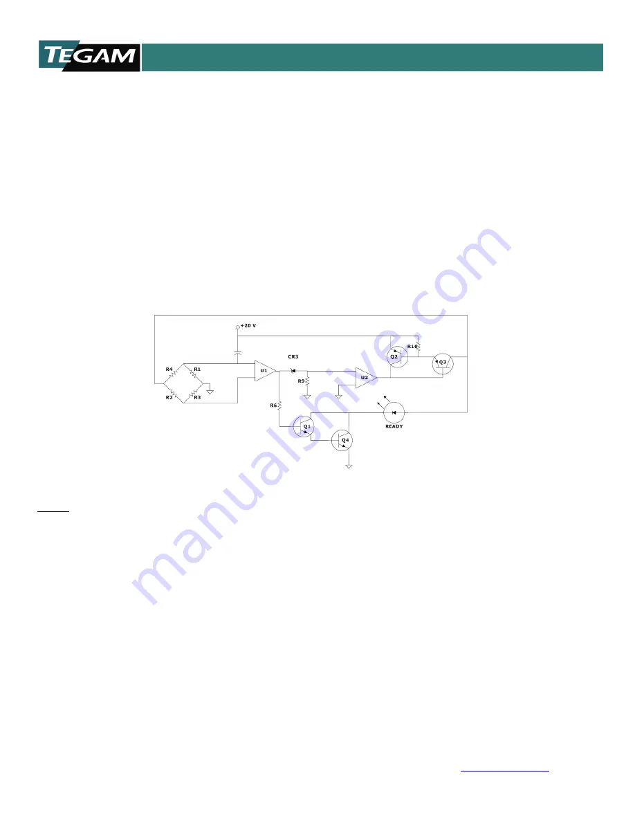
Refer to Figure 3.2 for the following discussions concerning the temperature control
circuit. The Model 1830A “bridge” balancer is composed of a controllable source that
allows current to flow through R
ref
and the bolometer. Identical precision instrument
amplifiers feed the bolometer voltage and the voltage across a reference resistor to a
servo-amplifier that has been adjusted for low offset.
Figure 3.2 - Simplified Schematic of the Model 1830A Heater Circuit
NOTE
The reference resistor is either 100 Ω or 200 Ω. Additionally, in some modes, the
reference resistance voltage is multiplied by a variable to produce a variable resistance feature.
At resistance other the 100 Ω or 200 Ω, the multiplication adds some uncer
tainty.
The servo amplifier controls the main supply transistor and therefore regulates power to the
combined reference/bolometer circuit.
The Model 1830A is designed to support NTC devices. When the bolometer voltage is higher than
desired, power is increased to heat the bolometer to decrease resistance. When the bolometer
voltage is lower than the reference resistor voltage, power is decreased. At balance, the
reference resistor voltage and the bolometer voltage match closely. Since the currents are the
same, the resistances also match closely.
The computation of power is determined by the change in voltage across the reference resistor.
When ZERO is pressed, the voltage across the reference resistor is stored in a combination of
DAC settings and softwa
re variables. This is done on both the “RF” channel and the
“Compensating” channel. For any subsequent reading, the actual values of the voltages are
used.


