— 30 —
SECTION 5
ELECTRICAL ADJUSTMENTS
5-1.
BASE UNIT SECTION
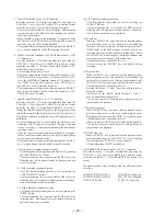
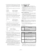
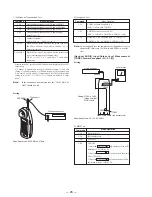
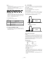
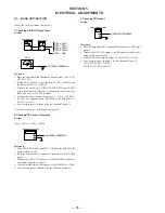
• Make the set in Test mode (see page 21)
1. Checking RX I&Q Output Level
Setting:
3. Checking TX Output
Setting:
Procedure:
1. Place the base unit in the Continuous Receive mode (CH1, LNA
ON, AGC ON).
2. Set the SSG frequency to the frequency on CH1 + 300 kHz, and
the RF output level to - 95 dBm.
3. Measure the output level of RXIN, RXIP, RXQN, and RXQP
with a level meter. At this time, confirm with an oscilloscope
that a sine wave of 300 kHz is output.
4. Confirm that the measured output level is -25.0 to -20.0 dB V.
IF IC501 was replaced (there is no ID data), the output level is
-26 dB V or less.
5. Also, execute steps 1 through 4 for the channels 10 and 20.
* For the frequency on each channel, see page 18.
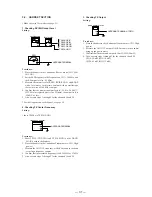
2. Checking TX Center Frequency
Setting:
• short: TP515
˜
TP567 (GND)
+
level meter
oscilloscope
–
+
–
TP558: RXIP
TP557: RXIN
TP556: RXQP
TP555: RXQN
TP567: GND
SSG
ANTENNA TERMINAL
+
frequency counter
ANTENNA TERMINAL
–
Procedure:
1. Short TP515 (TX DATA) and TP567 (GND) on the BASE MAIN
board in the base unit.
2. Place the base unit in the Continuous Transmit more (CH1, High
power).
3. Measure the ANT OUT frequency of the RF module in the base
unit using a frequency counter.
4. Coufirm that the measured frequency is 904.200 MHz ± 27kHz.
5. Also, execute steps 1 through 4 for the channels 10 and 20.
Procedure:
1. Place the base unit in the Continuous Transmit more (CH1, High
power).
2. Measure the ANT OUT output of the RF module in the base unit
using a peak power meter.
3. Confirm that the measured output is 30 mW (MIN 11 mW).
4. Also, execute steps 1 through 3 for the channels 10 and 20.
CH10: 30 mW (MIN 11 mW)
CH20: 30 mW (MIN 10 mW)
+
peak power meter
–
ANTENNA TERMINAL
Содержание SPP-A9171 - Cordless Telephone With Answering Machine
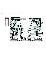
Страница 38: ...SPP A9171 41 42 6 4 SCHEMATIC DIAGRAM BASE MAIN SECTION 1 2 See page 33 for Note on Schematic Diagrams ...
Страница 39: ...SPP A9171 43 44 6 5 SCHEMATIC DIAGRAM BASE MAIN SECTION 2 2 See page 33 for Note on Schematic Diagrams ...
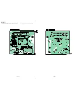
Страница 41: ...SPP A9171 47 48 6 7 SCHEMATIC DIAGRAM BASE KEY SECTION See page 33 for Note on Schematic Diagrams ...
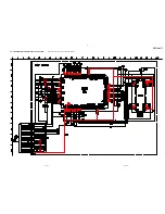
Страница 43: ...SPP A9171 51 52 6 9 SCHEMATIC DIAGRAM DISPLAY SECTION See page 33 for Note on Schematic Diagrams ...
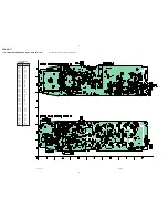
Страница 45: ...SPP A9171 55 56 6 11 SCHEMATIC DIAGRAM HAND MAIN SECTION See page 33 for Note on Schematic Diagrams ...

