background image

SPP-A9171

US Model

Canadian Model

SERVICE MANUAL

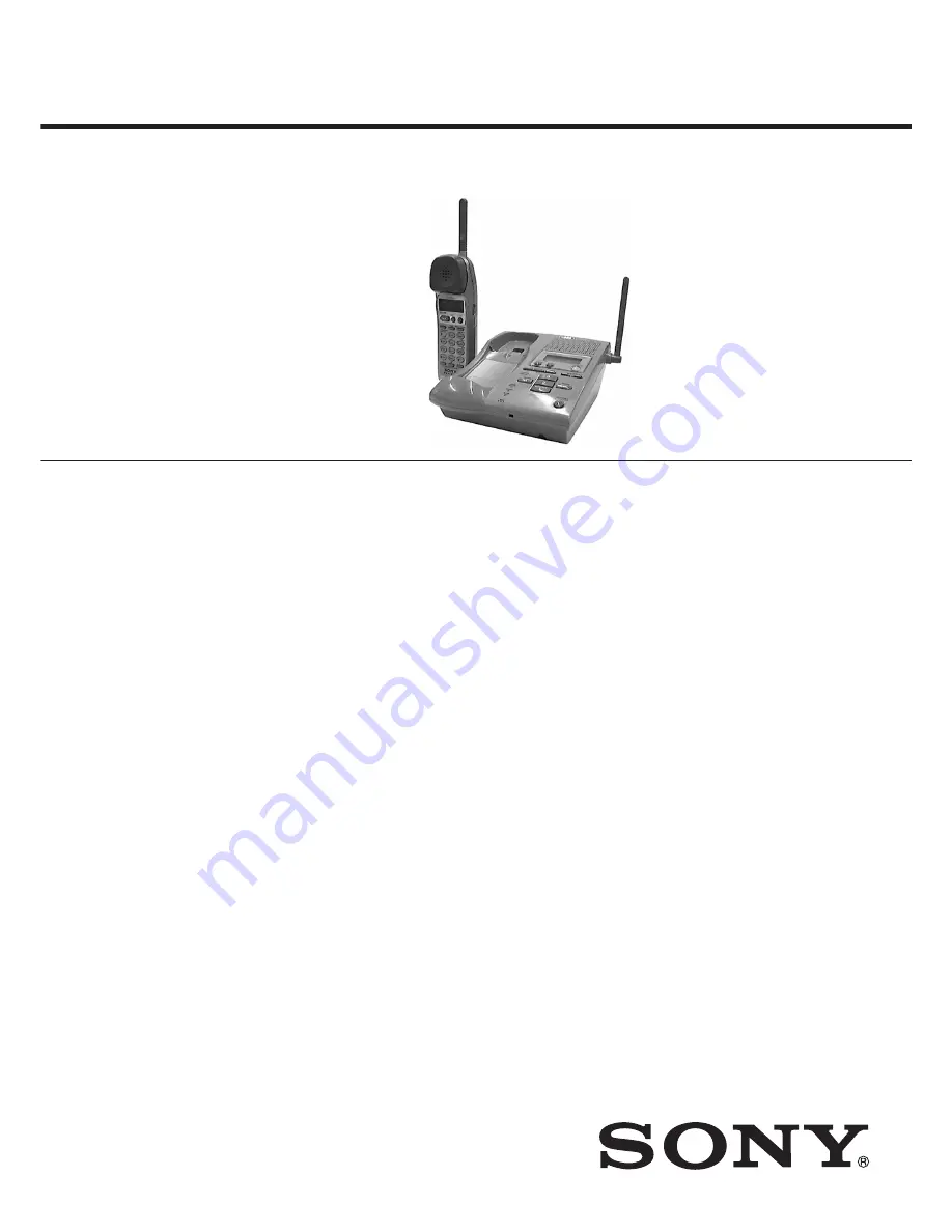
CORDLESS TELEPHONE

SPECIFICATIONS

General

Spread method

Direct-Sequence Spread-Spectrum

Access method

FDMA-TDD

Operation frequency

902 - 928 MHz

Operating channel

14 channels

Dial signal

Tone, 10 PPS (pulse) selectable

Handset

Power source

Rechargeable battery pack BP-T31

Battery charging time

Approx. 12 hours

Battery life

Standby: Approx. 7 days
Talk:

Approx. 6 hours

Dimensions

Approx. 2 

1

4

 x 7 

1

4

 x 2 

1

4

 inches (w/h/d),

antenna excluded
(approx. 56 x 183 x 55 mm)
Antenna: Approx. 3


inches

(approx. 75 mm)

Mass

Approx. 9.5 oz (approx. 270 g), battery
included

Base unit

Power source

DC 9V from AC power adaptor AC-T46

Battery charging time

Approx. 24 hours

Dimensions

Approx. 6 

3

 8

 x 2 

7

8

 x 8 

3

4

 inches (w/h/d),

antenna excluded
(approx. 160 x 71 x 222 mm)
Antenna: Approx. 4 

1

 2

 inches

(approx. 113 mm)

Mass

Approx. 1 lb 3 oz (approx. 540 g), wall
bracket excluded

Answering machine

Maximum recording time

About 18 minutes (at NORM (Long)
recording quality), using incorporated IC

Greeting message

Up to 4 minutes

Incoming message

Up to 4 minutes/message

Memo

Up to 4 minutes/message

Design and specifications are subject to
change without notice.

Ver 1.0  2000. 08

Содержание SPP-A9171 - Cordless Telephone With Answering Machine

Страница 1: ...x 56 x 183 x 55 mm Antenna Approx 3 inches approx 75 mm Mass Approx 9 5 oz approx 270 g battery included Base unit Power source DC 9V from AC power adaptor AC T46 Battery charging time Approx 24 hours Dimensions Approx 6 3 8 x 2 7 8 x 8 3 4 inches w h d antenna excluded approx 160 x 71 x 222 mm Antenna Approx 4 1 2 inches approx 113 mm Mass Approx 1 lb 3 oz approx 540 g wall bracket excluded Answe...

Страница 2: ...9 6 9 Schematic Diagram Disp Section 51 6 10 Printed Wiring Board Hand Main Section 53 6 11 Schematic Diagram Hand Main Section 55 6 12 IC Pin Functions 57 7 EXPLODED VIEWS 7 1 Handset Section 62 7 2 Base Unit Section 63 8 ELECTRICAL PARTS LIST 64 Notes on chip component replacement Never reuse a disconnected chip component Notice that the minus side of a tantalum capacitor may be damaged by heat ...

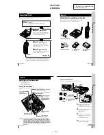
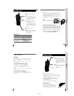
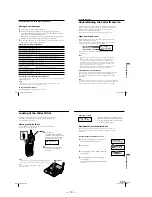
Страница 3: ...way from a personal computer Away from another cordless telephone Near a central location and on a level surface Away from heat sources such as radiators airducts and sunlight Away from noise sources such as a window by a street with heavy traffic Setting up the base unit Do the following steps Choose the best location Connect the base unit Choose the dialing mode Choose the best location Where yo...

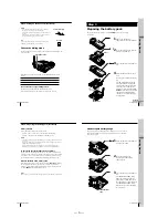
Страница 4: ... about Approx 6 hours when you use the handset continuously Approx 7 days when the handset is in standby mode Notes The battery pack will gradually discharge over a long period of time even if not in use If you leave the battery pack in the handset without charging it the battery pack will be completely discharged It may require several times of charging to recover to its full capacity While charg...

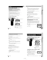
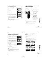
Страница 5: ...s you entered the phone number will be registered with 10 digits in the Caller ID list area code number If a call does not match one of the local area codes you entered the phone number will be registered with 11 digits in the Caller ID list 1 area code number Some regions of the country allow you to have more than one local area code Up to five local area codes can be entered in this phone 1 Pres...

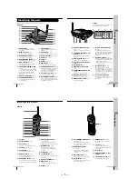
Страница 6: ...re is no space to record messages P appears when the power is turned on 4 VOL volume indicator Indicates the speaker volume The bars increase as the volume is turned up ql HANDSET LOCATOR button p 32 Allows you to page the handset w PLAY STOP MAILBOX 1 2 3 buttons p 43 Plays back the messages in each mail box wa DIAL MODE switch p 10 Selects pulse or tone dialing ws Hook for AC power adaptor cord ...

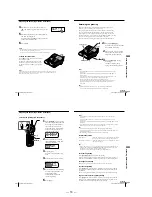
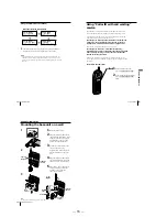
Страница 7: ...isplay and the phone cannot be used After E and BATTERY LOW go off you may be able to use the phone but the battery duration will be very short thus it is recommended that you fully charge the battery before next use continued Basics 24US Making calls continued Redialing 1 Press TALK and wait until TALK appears on the display 2 Press REDIAL PAUSE to redial the number last dialed Note If the number...

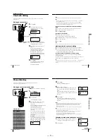
Страница 8: ...been entered is displayed next to 15th digit and then the all digits are displayed in two lines after about two seconds 28US Telephone Features You can dial a number by scrolling through the Phone Directory You can store up to 100 numbers Storing phone numbers and names Example to store SONY 123 4567 1 Press PGM 2 Press Jog Dial ENTER NAME appears 3 Enter the name using the dialing keys You can en...

Страница 9: ...gDialagain Thephonenumberwillbedialed Tips You may press TALK to make a call instead of doing steps 3 and 4 When the phone number of 17 digits or more has been entered is displayed next to 15th digit and then the all digits are displayed in two lines after about two seconds About the search order The names appear in the following order when you turn Jog Dial up or down Alphabetical order ABC XYZ y...

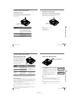
Страница 10: ...chine Features 36US Preparing the answering machine continued To record the greeting from the handset 1 Press REMOTE and wait until the answering machine function menu appears on the display If you hear five short error beeps and OUT OF RANGE appears on the display move closer to the base unit 2 Turn Jog Dial down to make REC GREETING flash and then press Jog Dial 3 Press Jog Dial You hear a long ...

Страница 11: ...cluding the greeting messages and memo If the remaining recording area becomes less than one minute F flashes on the display and the phone automatically switches to announcement only mode which does not record messages and the greeting will be switched to the pre recorded greeting Available time for recording at NORM Long sound quality If you wish to record more messages erase the existing message...

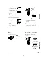
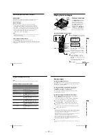
Страница 12: ... volume Set the VOL switch on the handset to H high M middle or L low Stop playback Press the mailbox button on the base unit again or press Jog Dial on the handset Replay the messages Press the mailbox button on the base unit again Skip to the next message Press SKIP QUICK on the base unit or SKIP 3 on the handset while the current message is playing Repeat the current message Press REPEAT REVIEW...

Страница 13: ...and the recorded memo is counted as a new message MIC Microphone MAILBOX 1 MAILBOX 2 MAILBOX 3 continued Answering Machine Features 48US Recording a memo continued To record a memo from the handset 1 Press REMOTE and wait until the answering machine function menu appears on the display If you hear five short error beeps and OUT OF RANGE appears on the display move closer to the base unit 2 Turn Jo...

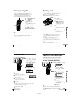
Страница 14: ...l not appear in the following cases OUT OF AREA when the call is made through a telephone company which does not offer Caller ID service including international calls PRIVATE when the call is blocked For privacy reasons many states allow callers the option to prevent his or her telephone data from being displayed on the other party s Caller ID display If the call is from an office which uses multi...

Страница 15: ...tory 1 Display the name and phone number you want to store from the Caller ID list see page 52 2 Confirm the number and press Jog Dial 3 Turn Jog Dial up to make PGM flash and press Jog Dial The cursor flashes at the end of the name Enter or change the name if necessary see page 29 4 Press Jog Dial The cursor flashes at the end of the phone number Enter or change the phone number if necessary see ...

Страница 16: ...s the two services Even though you now have a Caller ID with call waiting compatible phone unless you subscribe to the combined Caller ID with call waiting service you will not be able to see the name and number of the second caller When a new call comes in while you are talking the caller s name and or phone number of the new call appears on the display for about 20 seconds To switch to another c...

Страница 17: ...n board 4 Helical antenna Connector CN601 1 2 3 6 2 1 CABINET REAR HANDSET 2 2 HAND MAIN BOARD HANDSET 2 3 CABINET UPPER ASSY BASE UNIT 2 4 CABINET LOWER ASSY BASE UNIT 5 Base key board 6 Button FUNCTION 7 Button ANS 8 Lens 9 Cabinet Upper 4 Five screws BTP2 6x8 1 Two screws P3x10 3 Cabinet Lower assy 2 Two screws P3x10 5 Three screws BTP2 6x8 6 Base Main board 2 DSP board 3 Microphone board 7 Cab...

Страница 18: ...quested side is the slave when the RF link has been established 2 Initial Acquisition In order to establish the RF link between BASE UNIT and HANDSET both of BASE UNIT and HANDSET need to have the same system ID When power is applied to this system the system have to do Initial Acquisition in order to have the same system ID It is to exchange a parameter when the HANDSET is parked on the BASE UNIT...

Страница 19: ...If the BASE UNIT can not receive the A Frame of Heart beat from the HANDSET it become link error and the system become error recovery mode 4 Stand by Mode Operation 1 HANDSET When the HANDSET is the stand by mode sleep mode the HANDSET do the intermittent operation for power save because the HANDSET is the battery operation This process of stand by mode operation is as follows 10 sec 10 sec Heart ...

Страница 20: ...hment are as follows Fig 3 3 Link Establishment protocol Master TX Master RX Slave RX Slave TX Master Time Slot Trip Delay TX RX TX RX TX A V A V V V V A V A V Fig 3 4 Link Establishment Timing Chart 6 State Change Tarmination After the RF link between HANDSET and BASE UNIT was established a movement of each state State ON Hook OFF Hook PAGE Intercom etc is sent through supervisory bits 7 Error Re...

Страница 21: ...Control Test 1 When the IC501 Pin wg input PAEKP changes from L H to L during charge detection the IC501 Pin output CHRG_CTL will output H L to H only once 4 1 1 BASE UNIT Test Mode A 1 1 In test mode idling A and the P PULSE T TONE switch set to the P PULSE state pressing the HANDSET LOCATOR key changes the mode as shown below 2 Setting the P PULSE T TONE switch from P PULSE to T TONE in the BASE...

Страница 22: ...EPTION mode LNAON AGC MIN 1ch continuous RECEPTION mode LNA ON AGC OFF 10ch continuous RECEPTION mode LNA ON AGC MIN 10ch continuous RECEPTION mode LNA ON AGC OFF 20ch continuous RECEPTION mode LNA ON AGC MIN 20ch continuous RECEPTION mode LNA ON AGC OFF 1ch continuous transmission mode high power 1ch continuous transmission mode middle power 1ch continuous transmission mode low power 10ch continu...

Страница 23: ...e test mode 1 from the test mode idle state using the VOLUME keys Press the ANSWER key and the system enters the test mode 1 Call Arrival Detection Test mode Duringthe CallArrivalDetectionTest mode thecommunication line is in the open state the machine monitors the RING DET IC201 25 pin port 30 When the RING DET port is LOW the arrival call is present theANSWER LED lights up When the RING DET port...

Страница 24: ... set by pressing the GREETING REC button The communication line is closed and the DSPs enter the following state Microphone is muted speaker is turned on send is muted and receive is turned on 3 Speaker playback sound path setting The speaker playback sound path can be set by pressing the TIME button The communication line is opened and the DSPs enter the following state Microphone is muted speake...

Страница 25: ... is All 0 s 1 is All 1 s U is Counts up and D is Counts down Mode Operation 9 RECORDING QUALITY Slide Switch Test LCD 8 indication Select the test mode 8 from the test mode idle state using the VOLUME keys Press the ANSWER key and the system enters the test mode 8 RECORDING QUALITY Slide Switch Test mode The slide switch positions are judged from the LED indications as follows LONG PLAY ANSWER LED...

Страница 26: ...mmand Mode Operation One channel continuous send TX power HIGH One channel continuous send TX power Medium One channel continuous send TX power Low One channel continuous send TX power High Spread code 0 Channel increment 2 ch n 3 ch n 20 ch n 1 ch n When the PGM button is pressed the spread code is set 600 kHz n 300 kHz n 200 kHz n 100 kHz n 0 n Normal increments When the One ouch C is pressed wh...

Страница 27: ...vicing Perform measurement using the spectrum analyzer and jig antenna 4 5 1 RF Testing method Please follow the below instruction to perform RF test Setting Condition Connect a receiving antenna to RF INPUT of Spectrum analyzer and set the unit 10 cm 4 inches away from the receiving antenna Measuring tool Spectrum analyzer equivalent to HP8595E Jig Receiving antenna for Spectrum analyzer Check th...

Страница 28: ...RBW 1 MHz VBW 100 kHz Span 5 MHz Setting Test mode Continuous Transmit mode CH1 High Power Refer to Test Mode on page 21 9 8 7 6 5 4 3 2 1 1 2 3 4 5 6 7 8 9 18dB f 1 f 2 f0 f1 f2 PN Tr A 10dB Transmission Wave CENTER 904 2 MHz RBW 30 kHz SPAN 5 000 MHz SWP 50 0 msec 903 392 MHz MKR 16 00 dBm 903 392 MHz MKR 16 00 dBm ATTEN 10 dB RL 0 dBm 10 dB VBW 30 kHz Fig 1 CENTER 904 2 MHz RBW 30 kHz SPAN 5 00...

Страница 29: ...BASE UNIT MIN 18 dBm at High power Include location loss Measurement Measure peak level by Spectrum analyzer CENTER 903 600 MHz RES BW 1 0 MHz SPAN 5 000 MHz SWP 20 0 msec 903 587 MHz MKR 3 67 dBm AT 10 dB 0 dBm REF PEAK LOG WA SB SC FC CORR PLOTTER ADRS 10 dB VBW 100 kHz 0 ...

Страница 30: ...e page 18 2 Checking TX Center Frequency Setting short TP515 TP567 GND level meter oscilloscope TP558 RXIP TP557 RXIN TP556 RXQP TP555 RXQN TP567 GND SSG ANTENNA TERMINAL frequency counter ANTENNA TERMINAL Procedure 1 Short TP515 TX DATA andTP567 GND on the BASE MAIN board in the base unit 2 Place the base unit in the Continuous Transmit more CH1 High power 3 Measure the ANT OUT frequency of the R...

Страница 31: ... short TP820 TP814 GND level meter oscilloscope TP804 RXIP TP803 RXIN TP802 RXQP TP801 RXQN TP814 GND SSG ANTENNA TERMINAL frequency counter ANTENNA TERMINAL peak power meter ANTENNA TERMINAL TP812 Procedure 1 Short TP820 TX DATA and TP814 GND on the HAND MAIN board in the handset 2 Place the handset in the Continuous Transmit more CH1 High power 3 Measure theANT OUT frequency of the RF module in ...

Страница 32: ...utput TP555 RXQN TP556 RXQP TP557 RXIN TP558 RXIP level meter Chcking RX I Q Output Level short TP515 TP567 GND Checking TX Center Frequency TP820 short TP820 TP814 GND Checking TX Center Frequency ANTENNA TERMINAL SSG Checking RX I Q Output Level frequency counter Checking TX Center Frequency peak power meter Checking TX Output TP801 RXQN TP802 RXQP TP803 RXIN TP804 RXIP level meter Chcking RX I ...

Страница 33: ...ions may be noted due to normal produc tion tolerances Circled numbers refer to waveforms Signal path N RX O TX P bell Note on Printed Wiring Boards Note X parts extracted from the component side b Pattern from the side which enables seeing a Through hole Indication of transistor Waveforms BASE UNIT SECTION 4 Vp p 9 6 MHz 1 IC501 5 OSCI HANDSET SECTION 4 Vp p 9 6 MHz 1 IC401 5 OSCI Note The compon...

Страница 34: ...UT VCC TEST SCL SDA NC NC NC GND HAND MAIN Board IC402 AT24C32N 10SI 1 8 TR HAND MAIN Board IC403 TC74VHC86FT EL START STOP LOGIC DATA WORD ADDRESS COUNTER X DECODER DEVICE ADDRESS COMPARATOR LOAD COMP SERIAL CONTROL LOGIC DATA RECOVERY H V PUMP TIMING D OUT ACK LOGIC Y DECODER EEPROM SERIAL MUX 1 2 3 4 5 6 7 8 D OUT D IN R W LOAD INC EN A0 A1 A2 VSS VCC WP SCL SDA 1 1A 2 1B 3 1Y 4 2A 5 2B 6 2Y 7 ...

Страница 35: ...Q TADACK ASICREQ ASICACK DATA BUSS0 DATA BUSS1 DATA BUSS2 DATA BUSS3 RING DET Q601 BUF STOP RESET RIP BRANCHP OHP IC501 ASIC LINEIN SPKROP LINEO SP901 SPEAKER FIL Q902 IC351 DSP CODEC SW501 DIAL MODE T P TONE PULSE KEYPADR2 KEYPADR3 SW CTL I2C DATA I2C CLK IC502 EEPROM SDA SCL SPOUTP SPOUTN HSOUT HMIN MIC1 MIC Q901 AMP MIN X351 4 096MHz XIN XOUT CIDIP CIDIN LIN LOUT IC202 SW IC352 FLASH MEMORY DGP...

Страница 36: ...TCH D404 407 D408 409 421 ILLUMINATION LCD BACK LIGHT TX RX BELL 25 77 22 23 5 6 88 RESTIP 24 4 5 79 95 57 60 93 96 7 6 12 13 13 12 6 21 18 97 98 94 38 39 47 46 72 71 70 69 68 87 89 66 80 67 90 83 82 81 92 84 23 22 21 19 18 7 6 16 24 17 5 10 11 12 2 4 9 53 58 11 8 ANT1 ANTENNA RFU801 RF UNIT RXIP RXIN RXQP RAQN RXEN TXDATA TXEN LNAATTN TXPWR0 TXPWR1 AGC SYNDATA REFOSC SYNCLK SYNSTB SYNEN RXIP RXIN...

Страница 37: ... 3 PRINTED WIRING BOARD BASE MAIN SECTION See page 33 for Note on Printed Wiring Board and Semiconductor Location 8 9 A B TO BASE KEY BOARD Page 46 TO BASE KEY BOARD Page 46 TO DSP BOARD Page 51 5 P D104 D105 D103 D102 ...

Страница 38: ...SPP A9171 41 42 6 4 SCHEMATIC DIAGRAM BASE MAIN SECTION 1 2 See page 33 for Note on Schematic Diagrams ...

Страница 39: ...SPP A9171 43 44 6 5 SCHEMATIC DIAGRAM BASE MAIN SECTION 2 2 See page 33 for Note on Schematic Diagrams ...

Страница 40: ...ION See page 33 for Note on Printed Wiring Board Page 39 Page 39 Ref No Location D301 E 3 D302 B 1 D303 C 3 D304 E 3 D305 E 3 D306 A 5 D307 A 6 D308 A 6 D309 A 6 D310 A 7 D311 D 1 D312 E 2 D313 D 1 D314 E 1 Q301 E 5 Q302 B 7 Q303 C 6 Semiconductor Location ...

Страница 41: ...SPP A9171 47 48 6 7 SCHEMATIC DIAGRAM BASE KEY SECTION See page 33 for Note on Schematic Diagrams ...

Страница 42: ...SPP A9171 49 50 6 8 PRINTED WIRING BOARD DISPLAY SECTION See page 33 for Note on Printed Wiring Board Page 40 1 678 526 1 678 526 C385 C386 ...

Страница 43: ...SPP A9171 51 52 6 9 SCHEMATIC DIAGRAM DISPLAY SECTION See page 33 for Note on Schematic Diagrams ...

Страница 44: ... 6 D205 B 5 D206 B 4 D207 B 6 D208 B 6 D209 B 6 D401 A 2 D404 E 6 D405 E 6 D406 E 5 D407 E 5 D408 E 2 D409 F 2 D410 B 4 D411 F 1 D412 E 1 D414 A 3 D415 A 4 D416 F 2 D417 F 2 D418 E 2 D419 E 2 D421 E 2 D601 A 7 D801 A 1 IC201 B 5 IC401 B 2 IC402 B 3 IC403 B 4 Q201 B 5 Q202 B 5 Q203 B 5 Q204 B 6 Q402 E 3 Q404 F 1 Q405 B 6 Q601 A 6 Semiconductor Location ...

Страница 45: ...SPP A9171 55 56 6 11 SCHEMATIC DIAGRAM HAND MAIN SECTION See page 33 for Note on Schematic Diagrams ...

Страница 46: ... capacitor Analog power supply Line driver output DAC channel Analog 0V power supply Positive speaker driver output DAC channel Negative speaker driver output DAC channel Not used open Digital 0V power supply Digital power supply 2 7 5 5 Volts Analog 0V power supply Pin No Pin Name I O Function 51 52 53 54 55 56 57 58 59 60 61 62 63 64 65 66 67 68 69 70 71 72 73 74 75 76 77 78 79 80 81 82 83 84 85...

Страница 47: ... used open HAND BASE select input VDD supply to pad ring VSS supply to pad ring Not used open Not used open VDD supply to core VSS supply to core Not used open Clock signal output to the EEPROM Two way data bus with the EEPROM ART input Park input active low on base station active high on handset ART output Frame sync Serial data input Serial data output Main clock input Not used open Analog 0V po...

Страница 48: ...rectional control LCD data Keypad bidirectional control LCD data Keypad bidirectional control LCD data Keypad bidirectional control LCD data Not used open VSS supply to core VDD supply to core Not used open VSS supply to pad ring VDD supply to pad ring LNA select Receive enable Synthesizer data 9 6 MHz clock used by synthesizer Synthesizer clock Synthesizer strobe Synthesizer power VDD supply to A...

Страница 49: ...O I I O I I I O O O I I O I O O Ground Main clock output Main clock input Reset signal input TADuC ACK output TADuC REQ output Test pin for out going test TADuC power down input ASIC REQ input ASIC TADuC data bus DSP serial clock output DSP serial data input DSP serial data output DSP ACK input ASIC ACK input DSP CS output DSP power down output DSP reset output DSP read write output N C RELAY driv...

Страница 50: ...ON 1 3 034 812 01 PAD EAR 2 3 014 329 01 CUSHION SP 3 X 3377 753 1 HINGE ASSY 4 3 034 810 01 SPRING LEAF 5 3 040 204 11 SPACER FLEXIBLE 6 3 034 817 11 PANEL LCD 7 3 034 814 11 CABINET FRONT 8 3 033 764 01 CUSHION MIC 9 1 771 617 11 SWITCH RUBBER KEY 10 3 224 638 01 SHEET CU LCD 11 3 034 821 01 HOLDER LCD 12 A 3673 091 A HAND MAIN BOARD COMPLETE 13 3 039 837 01 SHEET H S REAR 14 3 034 820 01 BUTTON...

Страница 51: ... Ref No Part No Description Remarks 67 X 3379 140 1 CABINET LOWER ASSY 68 3 037 081 01 PLUG ANTENNA 69 A 3622 469 A BASE MAIN BOARD COMPLETE 70 A 3673 094 A DSP BOARD COMPLETE 71 3 223 526 01 SHEET ADHESIVE FOR PANEL 72 3 226 180 01 SHEET CU BASE 73 3 048 690 01 SHEET DIFFUSION 74 3 226 059 01 SHEET LCD 75 3 226 179 01 CUSHION 76 3 224 639 01 CUSHION 77 3 226 433 01 CUSHION RUBBER A SP901 1 505 72...

Страница 52: ... 470 5 1 16W R311 1 216 827 11 METAL CHIP 3 3K 5 1 16W R312 1 216 839 11 METAL CHIP 33K 5 1 16W R313 1 216 827 11 METAL CHIP 3 3K 5 1 16W R314 1 216 839 11 METAL CHIP 33K 5 1 16W R315 1 216 827 11 METAL CHIP 3 3K 5 1 16W R316 1 216 839 11 METAL CHIP 33K 5 1 16W SWITCH S301 1 572 381 21 SWITCH KEY BOARD REC S302 1 572 381 21 SWITCH KEY BOARD PLAY S303 1 572 381 21 SWITCH KEY BOARD TIME S304 1 572 3...

Страница 53: ...0 16V C617 1 162 964 11 CERAMIC CHIP 0 001uF 10 50V C618 1 162 964 11 CERAMIC CHIP 0 001uF 10 50V C619 1 164 227 11 CERAMIC CHIP 0 022uF 10 25V C621 1 115 467 11 CERAMIC CHIP 0 22uF 10 00 10V C622 1 164 227 11 CERAMIC CHIP 0 022uF 10 25V C632 1 115 156 11 CERAMIC CHIP 1uF 10V C701 1 162 970 11 CERAMIC CHIP 0 01uF 10 25V C901 1 126 177 11 ELECT 100uF 20 10V C902 1 126 177 11 ELECT 100uF 20 10V C903...

Страница 54: ...ISTOR 2SC1623 L5L6 Q901 8 729 230 49 TRANSISTOR 2SC2712 YG RESISTOR 0R101 1 260 079 11 CARBON 22 5 1 2W R102 1 216 831 11 METAL CHIP 6 8K 5 1 16W 0R103 1 219 625 11 METAL OXIDE 22K 5 1W R104 1 216 826 11 METAL CHIP 2 7K 5 1 16W R105 1 216 839 11 METAL CHIP 33K 5 1 16W R107 1 216 810 11 METAL CHIP 120 5 1 16W R108 1 216 833 11 METAL CHIP 10K 5 1 16W R109 1 216 837 11 METAL CHIP 22K 5 1 16W R110 1 2...

Страница 55: ...P 470 5 1 16W R506 1 216 817 11 METAL CHIP 470 5 1 16W R507 1 216 817 11 METAL CHIP 470 5 1 16W R508 1 216 845 11 METAL CHIP 100K 5 1 16W R509 1 216 833 11 METAL CHIP 10K 5 1 16W R510 1 216 833 11 METAL CHIP 10K 5 1 16W R511 1 216 817 11 METAL CHIP 470 5 1 16W R512 1 216 801 11 METAL CHIP 22 5 1 16W R513 1 216 864 11 METAL CHIP 0 5 1 16W R514 1 216 864 11 METAL CHIP 0 5 1 16W R515 1 216 817 11 MET...

Страница 56: ...MIC CHIP 33PF 5 50V C377 1 162 921 11 CERAMIC CHIP 33PF 5 50V C378 1 162 921 11 CERAMIC CHIP 33PF 5 50V C379 1 162 921 11 CERAMIC CHIP 33PF 5 50V C380 1 162 921 11 CERAMIC CHIP 33PF 5 50V C381 1 162 921 11 CERAMIC CHIP 33PF 5 50V C382 1 162 921 11 CERAMIC CHIP 33PF 5 50V C384 1 162 921 11 CERAMIC CHIP 33PF 5 50V C385 1 163 011 11 CERAMIC CHIP 1500P 10 50V C386 1 163 299 11 CERAMIC CHIP 33P 5 50V C...

Страница 57: ...11 CERAMIC CHIP 0 0082uF 10 25V C614 1 164 174 11 CERAMIC CHIP 0 0082uF 10 25V C616 1 162 923 11 CERAMIC CHIP 47PF 5 50V C617 1 104 851 11 TANTAL CHIP 10uF 20 00 10V C619 1 162 919 11 CERAMIC CHIP 22PF 5 50V C620 1 162 921 11 CERAMIC CHIP 33PF 5 50V C621 1 115 565 11 CERAMIC CHIP 2 2uF 10 10V C622 1 162 921 11 CERAMIC CHIP 33PF 5 50V C623 1 107 682 11 CERAMIC CHIP 1uF 10 16V C624 1 163 239 11 CERA...

Страница 58: ...IP 470 5 1 16W R423 1 216 817 11 METAL CHIP 470 5 1 16W R424 1 216 845 11 METAL CHIP 100K 5 1 16W R425 1 216 845 11 METAL CHIP 100K 5 1 16W R426 1 216 817 11 METAL CHIP 470 5 1 16W R427 1 216 296 91 SHORT 0 R428 1 216 809 11 METAL CHIP 100 5 1 16W R429 1 216 805 11 METAL CHIP 47 5 1 16W R430 1 216 817 11 METAL CHIP 470 5 1 16W R433 1 216 864 11 METAL CHIP 0 5 1 16W R434 1 216 817 11 METAL CHIP 470...

Страница 59: ... 1 473 475 61 ADAPTOR AC AC T46 1 528 976 11 BATTERY NI CD BP T31 1 696 453 21 CORD WITH MODULAR PLUG LINE 1 696 454 11 CORD WITH MODULAR PLUG LINE 3 012 379 31 TAPESTRY CASE 3 043 181 01 STICKER ATTENTION CHARGE US 3 044 346 01 STICKER ATTENTION CHARGE CND 3 223 523 11 MANUAL INSTRUCTION ENGLISH US 3 223 523 21 MANUAL INSTRUCTION SPANISH US 3 223 523 31 MANUAL INSTRUCTION ENGLISH CND 3 223 523 41...

Страница 60: ...SPP A9171 72 Sony Corporation Audio Entertainment Group 2000H16093 1 Printed in Japan 2000 8 Published by General Engineering Dept 9 927 982 11 ...

Отзывы: