background image

6-6

DSC-H50_ADJ

4.

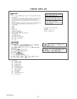
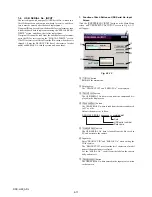
Precautions When Using Pattern Box

1) It takes about 30 minutes for pattern box to stabilize its brightness.

Turn on the pattern box 30 minutes before the adjustment starts.

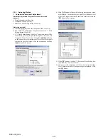
2) Make arrangement so that the outside light does not enter the chart surface in the pattern box.

Also, place a board between chart and camera, and make a hole at the lens part of the board so that the camera is not reflected in the
shot image screen.
(Adjustment may not be performed correctly due to the influence of outside light.)

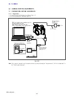
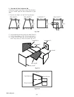
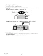
Example 1:

Place a box to block a section between pattern box and camera.

Fig. 6-1-6

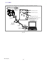
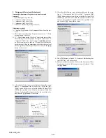
Example 2:

Place a board having a hole in front of the camera and cover the pattern box and camera with a blackout curtain

Fig. 6-1-7

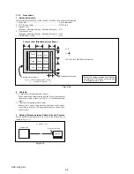
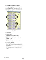
3) Control of color chart

The color chart will fade if it is exposed to direct sunlight or strong light.
Since the fading of color chart progresses even with the light in the pattern box, remove and store the color chart when it is not used.
Remove the color chart and store it.
Store the color chart in a place not exposed to direct light, avoiding high temperature and humidity.
Use the color chart for about three years, and afterward replace it with a new chart.

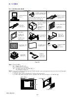
Pattern box

Front of the lens

Make the hole of the same
size as the lens. 

Make the hole of the same
size as the pattern box. 

L = About 7 cm

L

Camera

Pattern box

Front of the lens

Board that opens hole
to lens part

L = About 7 cm

L

Camera

Cover with a blackout curtain

Содержание DSC-H50

Страница 1: ...l previously issued DI08 234 SERVICE MANUAL Ver 1 2 2008 09 DSC H50_L2 9 852 286 81 US Model Canadian Model AEP Model UK Model E Model Australian Model Hong Kong Model Chinese Model Korea Model Argentine Model Brazilian Model Thai Model Japanese Model Tourist Model LEVEL 2 Change of Repair Parts DSC H50 RMT DSC2 ...

Страница 2: ...6 LCD SECTION A 2 CK 198 Board HELP11 1 4 Claw 1 6 1 14 1 3 2 7 14 2 8 A 2 CK 198 Board 2 CK 198 Board HELP11 1 4 Claw 1 6 1 14 1 3 2 7 1 2 7 1 2 8 2 8 Page 5 REPAIR PARTS LIST 5 1 EXPLODED VIEWS Before change After change 5 7 Changed portion 5 1 6 LCD SECTION 5 1 6 LCD SECTION A 14 254 255 256 257 A 1 254 255 256 257 ...

Страница 3: ...F7 D D C B L _ R S E7 V B U S _ I N D10 X M S _ I N G5 X E X T _ I N D9 X P W R _ O N 3 D8 X P W R _ O N 2 D7 X P W R _ O N 1 C10 X P W R _ O F F D6 X R E S E T _ R E Q D5 X N A N D _ R E S E T C9 X S Y S _ R E S E T C7 S O C6 S I C8 S C K C5 X C E A 1 0 TEST2 B 1 0 DDC1P8_RF B 9 DDC1P8_INM A 9 DDC1P8_PG A 8 DDC1P8_LX B 8 DDC1P8_PWR B 6 DDC1P8_VFB R051 XX R 0 3 1 1 k R 0 3 2 1 k C 0 6 5 X X 0 4 3 ...

Страница 4: ...2 AC23 IOVDD IOVDD GND GND IOVDD GND IOVDD IOVDD GND GND LENS CONTROL MOD 1 5 CPU CAMERA DSP AV SIG C212 XX C211 XX C213 XX D_3 1V D_3 1V IC211 PRX515103 V4 V5 R4 R5 B16 L14 AE24 AF24 AB22 AC23 IOVDD IOVDD GND GND IOVDD GND IOVDD IOVDD GND GND LENS CONTROL MOD 1 5 CPU CAMERA DSP AV SIG 2 4 C243 0 1u AB12 AB11 AE17 AC17 PI AVSS_PI AVCC_PI CCD1_IOVDD CCD2_IOVDD A_3 1V 2 4 C243 XX AB12 AB11 AE17 AC17...

Страница 5: ... 10 Location F 6 to G 7 SY 201 BOARD 6 10 Location F 6 to G 7 SY 201 BOARD 6 10 Location E 10 to F 11 SY 201 BOARD 6 10 Location E 10 to F 11 C390 0 1u C389 0 1u C321 0 1u C322 XX C325 0 1u C326 0 1u C385 0 1u C387 0 1u R C382 XX C395 22u 1 2 3 L312 XX M_13V C390 0 1u C389 XX C321 XX C322 XX C325 0 1u C326 XX C385 0 1u C387 XX R C382 XX C395 XX 1 2 3 L312 XX M_13V ...

Страница 6: ...0 G 2 MD_EN0 E 9 MD_IN1 F 9 MD_BR1 G 9 MD_EN1 G 7 xMD_PS V C C A 3 K1 V C C A 3 K6 G N D A 3 K7 G N D A 3 K10 O P _ I P 0 H2 G 4 TEST CL509 0 6 2 8 3 1 0 7 3 0 C522 0 1u 0 047u C532 0 047u 2 2 2 3 2 4 2 5 2 6 2 7 2 8 DGND LPFAIN1 DVcc CLK LPFBIN1 DATA AGND 3 1 2 8 C512 1u C504 XX A_3 1V V 3 V 4 PITCH YAW PITCH YAW C503 XX C507 XX 0 1u 10V A 1 PGND E 1 PGND A 1 0 PGND E 1 0 PGND F 1 DVCC F 1 0 DGND...

Страница 7: ...IST Page Before change After change 5 12 Ref No Part No Description Ref No Part No Description CAPACITOR C044 1 100 611 91 CERAMIC CHIP 22uF 20 6 3V C064 1 125 777 11 CERAMIC CHIP 0 1uF 10 10V C209 1 125 777 11 CERAMIC CHIP 0 1uF 10 10V C211 1 125 777 11 CERAMIC CHIP 0 1uF 10 10V C213 1 125 777 11 CERAMIC CHIP 0 1uF 10 10V C243 1 125 777 11 CERAMIC CHIP 0 1uF 10 10V C249 1 100 611 91 CERAMIC CHIP ...

Страница 8: ...100 611 91 CERAMIC CHIP 22uF 20 6 3V C503 1 125 777 11 CERAMIC CHIP 0 1uF 10 10V C504 1 165 908 11 CERAMIC CHIP 1uF 10 10V C507 1 125 777 11 CERAMIC CHIP 0 1uF 10 10V C522 1 125 777 11 CERAMIC CHIP 0 1uF 10 10V C603 1 165 989 11 CERAMIC CHIP 10uF 10 6 3V C619 1 165 908 11 CERAMIC CHIP 1uF 10 10V DIODE D601 6 501 947 01 DIODE MA2S1110G8S0 RESISTOR R601 1 218 929 11 RES CHIP 10 5 1 16W SY 201 BOARD ...

Страница 9: ... or dotted line with mark 0 are critical for safety Replace only with part num ber specified Les composants identifiés par une marque 0 sont critiques pour la sécurité Ne les remplacer que par une pièce portant le numéro spécifié DSC H50 RMT DSC2 Photo Black DIGITAL STILL CAMERA US Model Canadian Model AEP Model UK Model E Model Australian Model Hong Kong Model Chinese Model Korea Model Argentine ...

Страница 10: ... USB communication USB communication Hi Speed USB USB 2 0 compliant LCD screen LCD panel 7 5cm 3 0type TFT drive Total number of dots 230 400 960 Å 240 dots Finder Panel 0 5cm 0 2type color Total number of dots Approx 200 000 dots equivalent Power general Power Rechargeable battery pack NP BG1 3 6V NP FG1 not supplied 3 6V AC LS5K AC Adaptor not supplied 4 2V Power consumption during shooting LCD ...

Страница 11: ...owing safety checks before releasing the set to the customer ATTENTION AU COMPOSANT AYANT RAPPORT À LA SÉCURITÉ LES COMPOSANTS IDENTIFÉS PAR UNE MARQUE 0 SUR LES DIAGRAMMES SCHÉMATIQUES ET LA LISTE DES PIÈCES SONT CRITIQUES POUR LA SÉCURITÉ DE FONCTIONNEMENT NE REMPLACER CES COMPOSANTS QUE PAR DES PIÈSES SONY DONT LES NUMÉROS SONT DONNÉS DANS CE MANUEL OU DANS LES SUPPÉMENTS PUBLIÉS PAR SONY Unlea...

Страница 12: ...etailed code of the problem 0 0 3 2 C Repaired by Refer to 1 2 3 Self diagnosis Code Table Indicates the appropriate step to be taken E g 13 Format the Memory Stick Duo 32 Turn on power again Block Detailed Code Blinks at 3 2 Hz C Corrected by customer E Corrected by service engineer LCD screen 1 1 PRECAUTION ON REPLACING THE SY 201 BOARD DESTINATION DATA When you replace to the repairing board th...

Страница 13: ... Turn the power off and on again Retry turn the power on by the power switch If it does not recover check the focus reset sensor of lens block pin wj of CN401 on the SY 201 board If it is OK check the focus motor drive IC IC401 on the SY 201 board Retry turn the power on by the power switch Check the zoom reset sensor of lens block pin qj of CN401 on the SY 201 board if zooming is performed when t...

Страница 14: ... Format in Internal Memory Tool A new folder is created on the Memory Stick Duo and all the data will be copied to it You cannot choose a specific folder and copy images to it The Print order marks on the images are not copied Copy This item does not appear when a Memory Stick Duo is inserted in the camera Formats the internal memory Note that formatting permanently erases all data in the internal...

Страница 15: ...Data writing method 1 Connect the PC to the camera USB mode Mass Storage and switch the driver to the Sony Seus USB Driver 2 Start the Write Enable Tool and the SeusEX 3 Click the Activate Write Enable Mode button of the Write Enable Tool 4 Upon completion of the setting change the following message will be displayed 5 Return the driver to the original one and connect the PC to the camera USB mode...

Страница 16: ... t s w 64 4F S J B M P V i ZY oM b ý w4 Xtx w U V oMsMwp X õ t Ö b AUK b o 6 4 4 3 P 1 6 5 æ l o X i M ó ótmMo w tÆéùU ahqV óU V hØt rOr h MTQ pV Ô æM b ótmMox Ì t L o M b Ô w tÆéùU ahqV hØt çÑ Õ Äq w ÈU Ô p Ó b w È w Ôt lo0 ü S Æéùw ahÒé w ü ÆéùwÄI Å Ô b 0 0 3 2 C 0 ü Å 0 MOw Mt ü K K K ÝÞæ µÂ K K K o Ö Úb Òé ü ÄI Å Ó Sl p0 ϵ ï Ç p 0 Ãá Ñ Ú Ä b h Ø C 3 2 00 ...

Страница 17: ...Y w ü 4Y w èï s8 è ï Ì Î Ä 1 5 èï Ì Î Ä 8 Ûµ w Ñå áwF F wF U h Å 0 MO º ÝÞæ Ñ Ú Äb ÝÞæ µÂ Ãá Ñ Ú Äb ý M ÝÞæ µÂ Ãá t õb F ºw ÝÞæ µÂ Ãá àÖb owÖ Ú hx ÝÞæ µÂ Ãá wà s b o Ö Úb â µ w o Ö Úb î sMÔùxèï Òé wÑ µæ Ä ï 4 X wjÐï Ub sZ yÑ µÞ æ 4 X U b â µ w o Ö Úb ÜØ ï â hqVt Ü b yèï Òé w Üæ Ä ï 4 X qj Ðï Ub sZ y ÜÞ æ 4 X Ub ü 4Y 4 X U hx õb ü 4Y 4 X U hx õb ü 4YÒé w çÉ 1 5 4 X eg ejÐï Ub sZ y 1 5 8 S ï 4 X4 w ...

Страница 18: ... æ Ä b tx q2pz ßï ç z w b æ Ä x oU sM Ot Xi M Ð º ÝÞæ tGå hhþ zÝÞæ µÂ Ãá t Å Ð b 1 FüsíV0 wK ÝÞæ µÂ Ãá tÖ 2 ïÄé çØ ïw p Ð z w b º ÝÞæ wà Ub o Ð b qMOÝ U Ô 3 p îæ z w b Ð Uîæ Ð b t x q 3 p z ßï ç z w z b FütF hÌ Âæ Xi M w sMÌ Âæ ohþÑ ç Ð b qz Ì Âæ wh à 8ùpVsTlh z à b S f UK b hþ qw Ð xpV d à Рo z º ÝÞæ ºwà x_ d º ÝÞæ wº0 b txz Ð t ÝÞæ µÂ Ãá T xc z º ÝÞæ À ç w Ñ Ú Ä æloXi M à Рb q ÝÞæ µÂ Ãá ºtý MÑ...

Страница 19: ... srt º ÝÞæ à VíbÔùtx w Ì t Ëb AUK b w Ëtx V DÀ ç 8 S J U F OBC M F5PP M FYF b Ví MO Ýåq1 ÚµµÄè Åå Ì 4 P O Z 4F VT 6 4 S JW FS t 8Q V DÀ çq4FVT 9 I b V DÀ çw Activate Write Enable Mode Ø ï æ b w ËU4 b q ÍwÝ U Ô b Åå Ì ití oz Ýåq1 ÚµµÄè b 1 t Z oSMhà Ýåwº ÝÞæt V Ýåq1 w r Ýåw o 0 tb Ýåw o 0 tb qt V Dw Ur b ...

Страница 20: ... up to the maximum 315 V potential There is a danger of electric shock by this high voltage when the capacitor is handled by hand The electric shock is caused by the charged voltage which is kept without discharging when the main power of the unit is simply turned off Therefore the remaining voltage must be discharged as described below Preparing the Short Jig To preparing the short jig a small cl...

Страница 21: ... Board Cabinet Rear Section u SW 532 Board LCD Block u CK 198 Board u CK 199 Flexible Board 2 2 1 OVERALL SECTION uCabinet Rear Section uRetainer SW uSide Cabinet R Block 2 2 2 FRONT PANEL SECTION 1 uLoudspeaker 1 3cm uSY 201 Board uLens Block 2 2 4 FRONT PANEL SECTION 3 uControl Switch Block uFront Panel Block 2 2 3 FRONT PANEL SECTION 2 uBattery Holder Stroboscope Block uBattery Holder Block uST...

Страница 22: ... 1 to 1 10 2 Retainer SW 2 1 3 Side Cabinet R Block 3 1 to 3 2 HELP HELP EXPLODED VIEW HARDWARE LIST 1 2 2 10 1 9 Claw 1 10 1 3 2 10 1 8 1 1 2 10 1 5 23 76 1 6 23 76 1 7 1 4 Open the LCD panel 1 Cabinet Rear Section See Page 2 7 2 Retainer SW 3 Side Cabinet R Block 2 1 3 2 2 10 3 1 HELP01 HELP01 Front Panel Section 1 See Page 2 4 ...

Страница 23: ... Block 2 11 76 2 12 Claw 2 13 Claw 2 1 2 5 2 8 2 10 2 9 2 3 2 4 2 6 2 7 2 16 2 15 2 14 2 2 Claw 3 1 76 3 2 74 3 3 Claw HELP02 HELP04 HELP03 HELP03 Note High voltage cautions Discharging the Capacitor Short circuit between the two points with the short jig about 10 seconds To avoid the spark with the metal plate wrap the short jig with the insulation tape ST 194 Board R 1 k1 1 W Part code 1 215 869...

Страница 24: ...older Block 2 1 to 2 4 3 ST 195 Flexible Board 3 1 to 3 8 EXPLODED VIEW HARDWARE LIST C B C A B A 1 1 76 1 3 1 5 1 4 1 2 DC Lid 1 Battery Holder Stroboscope Block 2 Battery Holder Block 3 ST 195 Flexible Board 2 1 76 2 3 2 4 2 2 Claw 3 1 12 3 2 Claw 3 5 Claw 3 6 Claw 3 7 3 3 3 4 HELP06 HELP05 HELP08 HELP06 HELP07 Front Panel Section 3 See Page 2 6 3 8 ...

Страница 25: ...ntrol Switch Block 1 1 to 1 4 2 Front Panel Block 2 1 to 2 5 EXPLODED VIEW HARDWARE LIST SI 115 Flexible Board Attach SI 115 flexible board to microphone holder as shown in the figure Microphone Holder 2 1 76 2 3 76 1 1 76 1 3 Claw 2 2 1 4 2 4 2 5 1 Control Switch Block 2 Front Panel Block HELP03 1 2 ...

Страница 26: ...1 to 1 5 2 LCD Section 2 1 to 2 4 EXPLODED VIEW HARDWARE LIST 1 1 5 1 2 1 3 1 5 1 4 Claw 1 SW 532 Board 2 LCD Section See Page 2 8 2 2 12 Hinge Part 2 3 Claw 2 4 2 1 12 HELP10 HELP09 Hinge Part How to diassemble the Hinge Part Pass it through this point of Cabinet Rear Pass it through this point of Cabinet Rear ...

Страница 27: ...al order given 1 P Cabinet C Assy 470 1 1 to 1 9 2 CK 198 Board 2 1 to 2 8 EXPLODED VIEW HARDWARE LIST A A 1 1 1 14 1 P Cabinet C Assy 470 2 CK 198 Board 2 1 2 3 1 14 HELP11 HELP11 HELP11 HELP12 1 4 Claw 1 8 Claw 1 7 1 14 1 6 1 14 1 5 1 9 1 2 1 3 2 4 2 5 2 6 2 7 14 2 8 2 2 ...

Страница 28: ...sibility Dial In case of assembling the cabinet rear assy attach it after turning fully counterclockwise the visibility dial Be careful about the lever inside of the eye cup assy doesn t go over the EVF lever Eye Cup Assy Cabinet Rear Assy Bend the flexible board to the main body side at claws Lever EVF HELP02 EVF Claws Tape A 0 to 1mm 0 to 1mm ...

Страница 29: ...ELP03 HELP04 Harness Microphone Unit Lib Lib Microphone Holder Loudspeaker 1 3cm Cutout Cutout Lens Block Assy Lens Radiation Sheet Crease left point Attach covering the flexible board 0 to 1mm Harness Loudspeaker 1 3cm ...

Страница 30: ...E BATTERY TERMINAL BOARD Battery Terminal Board 1 Insert the battery terminal board into a slit in the BT holder to install The battery terminal holder are attached with the notch for installation Notch HELP05 Battery Terminal Board BT holder DC 111 Flexible Board Notch Battery Terminal Board ...

Страница 31: ...ing Points 4 Lib THE METHOD OF ATTACHMENT OF HARNESS HN 042 to HN 044 Solder three harnesses to ST 195 flexible board and ST 194 board Note Be careful about the colors of harnesses Attach ST 195 flexible board to ST base assy and insert three harnesses to lib deeply Note Be careful about the overlaps of harnesses Note Be careful not to damage the covering of harnesses Insert the harnesses in the a...

Страница 32: ...bs Pink Blue White Claw Claw Claw FL Cover Claw Cabinet Upper Pass three harnesses in lib Note Be careful about the overlaps of harnesses Pull up the popping up and straighten three harnesses Attach Cabinet Upper Attach FL cover ...

Страница 33: ... Board Harnesses Claw Claw ST Cover Claw Battery Holder Block BT Holder Cover Screw Attach ST cover Attach Capacitor holder and arrange three harnesses as shown in the figure Assemble Capacitor holder and BT holder cover with ST 194 board to Battery holder block and secure them with a screw Pull up the popping up and secure a screw ...

Страница 34: ...3 4 Screw Screw Boss Boss PL 051 Board Claw Attach Plunger solenoid to three pins while closing the popping up Note Be sure not to touch the copper leads or contacts Attach PL 051 board while positioning to two bosses and secure it with two screws Attach Solenoid retainer to two pins and secure it with a screw Solder two points ...

Страница 35: ...DSC H50_L2 HELP HELP08 HELP09 Harness HN 042 Pink Libs Harness HN 043 White Harness HN 044 Blue Flexible Adhesive Sheet Pink Blue White ...

Страница 36: ...HELP10 1 2 3 4 Hinge Assy 470 LCD Block Panel Side Front Side Pull out CK 199 flexible board from the underneath of hinge assy 470 and put it on the cabinet rear Insert hinge assy 470 to cabinet rear as shown in the figure Position hinge assy to two bosses and secure it with four screws Position CK 199 flexible board to the dowel and attach it to adhesive portion At this time make the free space t...

Страница 37: ...DSC H50_L2 HELP HELP11 HELP12 Flexible Slider Sheet CK 199 Flexible Board CK 199 Flexible Board CK 199 FLEXIBLE BOARD ARRANGEMENT Hinge Cover M Assy P Cabinet C Assy 470 CK 198 Board 1mm ...

Страница 38: ...DSC H50_L2 Link Link 3 BLOCK DIAGRAMS OVERALL BLOCK DIAGRAM 2 2 OVERALL BLOCK DIAGRAM 1 2 POWER BLOCK DIAGRAM 1 2 POWER BLOCK DIAGRAM 2 2 ...

Страница 39: ...D CLOCK HSYNC VSYNC XDD_SYS_RST U19 XCS_ PANEL XCS_ PANEL XCS_ PANEL XCS_FE XIC_211_3_SCK IC_211_3_SO IC_211_2_SO XIC_211_2_SCK IC_211_2_SO XIC_211_2_SCK IC_211_2_SO XIC_211_2_SCK AB13 AF12 AC12 H8 IC_211_YOUT V_LINE_OUT IC_211_YOUT IC_211_PBOUT IC_211_PROUT IC_211_YOUT IC_211_PBOUT IC_211_PROUT USB_DP USB_DM MSX_BS MSX_D0 MSX_D3 MSX_CLK G9 G6 F9 J9 F6 F5 F7 G5 E9 D9 E5 C4 D10 D1 D2 H1 H2 K1 K2 3 ...

Страница 40: ...C001 Q001 Q002 A23 V2 H9 H15 Y16 W20 JOG_A G16 B21 C10 XPWR_OFF G8 G3 T7 F6 BATT_SENS MS_PWR_ON AE7 K8 G9 H17 A24 G17 W12 AB18 IC_211_0_SO IC_211_0_SI XIC_211_0_SCK IC_211_0_SO IC_211_0_SI XIC_211_0_SCK 2 OVERALL 1 2 PAGE 3 1 D26 G19 STRB_CHG XSTRB_FULL STB_CHG_CNT STRB_ON K7 K6 C4 D9 X001 32 768kHz MODE_DIAL2 XPWR_LED XAE_LOCK XSHUT_SW MODE_DIAL1 XPWR_ON BRK S004 8 KEY_AD2 KEY_AD2 MODE_DIAL2 STRB...

Страница 41: ... 2 2 PAGE 3 4 B POWER 2 2 PAGE 3 4 D 2 5 BATT_SIG BATT_UNREG BATT_SIG BATT_UNREG REG_GND JK 371 FLEXIBLE BOARD DC 111 FLEXIBLE BOARD CN001 MULTI CONNECTOR 23 25 19 7 L009 DDC1P8_LX A8 DDC1P8_PWR B8 DDC1P8_VFB B6 D_1 85V L008 DDC1P2_LX A4 DDC1P2_VFB B2 D_1 25V CAM_3 5V LD03P4_OUT H3 D_1 5V LD01P5_OUT A6 DDR_1 8V LD01P8_OUT A7 BL_H DDCBL_VO F9 BL_L DDCBL_VL E10 USB_3 2V LD03P1U_OUT J5 MS_PWR_OUT F3 ...

Страница 42: ...PITCH SENSOR YAW SENSOR R254 GPS_13 W7 L303 L602 L302 C356 R407 R408 FB302 FB309 FB310 FB303 CCD SIGNAL PROCESS TIMING GENERATOR 6 10 Q303 7 5V DISCHARGE IC304 RSTB E11 G4 G3 RNF RNFS 2 3V REG 6 10 1 2 IC306 4 VDD Vout 3 2 8V REG 8 10 IC507 A_3 1V 2 8V D_1 85V D_3 1V M_5 0V XDD_SYS_RST XDD_SYS_RST XDD_SYS_RST XDD_SYS_RST PANEL_6 4V RESET VCC2 6 4V VCC 3V BL_H BL_L XIC_211_IC_503_RST VDD CE 1 4 Vou...

Страница 43: ...HARGEABLE BATTERY CK 199 FLEXIBLE BOARD LE 042 FLEXIBLE BOARD ST 195 FLEXIBLE BOARD JK 371 FLEXIBLE BOARD DC 111 FLEXIBLE BOARD PL 051 BOARD ST 194 BOARD SI 115 FLEXIBLE BOARD CK 198 BOARD CN713 MEMORY STICK CONNECTOR 2 30 1 29 CN002 2 38 1 1 28 39 1 28 CN001 CN002 J001 DC IN 2 26 27 28 1 25 CN001 CN001 MULTI CONNECTOR D002 AF ILLUMINATOR SELF TIMER D001 NIGHTSHOT D001 D002 SW 532 BOARD SIDE B FP ...

Страница 44: ...T 195 FLEXIBLE BOARD FLASH UNIT DC 111 FLEXIBLE BOARD BATTERY IN DC IN PL 051 BOARD STROBE PLUNGER FP 900 FLEXIBLE BOARD SY ST CONNECTION FP 901 FLEXIBLE BOARD SY SW CONNECTION SI 115 FLEXIBLE BOARD REMOTE CONTROL RECEIVER PB 052 FLEXIBLE BOARD PLAYBACK SLIDESHOW SWITCH SW 532 BOARD ZOOM SWITCH CONTROL SWITCH BLOCK SW60350 CONTROL SWITCH BLOCK LE 042 FLEXIBLE BOARD NIGHTSHOT AF ILLUMINATOR Link Li...

Страница 45: ...form Voltages and waveforms are measured between the measurement points and ground when camera shoots color bar chart of pattern box They are reference values and reference waveforms VOM of DC 10 M1 input impedance is used Voltage values change depending upon input impedance of VOM used Kinds of capacitor Case size External dimensions mm Yellow A A B B A B Fig a Video output terminal output wavefo...

Страница 46: ...Å CxÍÉç ÔÊ Ax å ï Bx µå ï Jx å ï µ wÖZ M Ôb CxÐTÊ y þ ÚEÊ Ä y t ôøþ xÍ ïØ µw å Ì ß Ä ø q hqVw 0 µ w ß Ã çÚç Ý Ö ïÐ ïµy 1 µ wÖ ïÐ ïµt y U s b 0 wæ hx0 ÇVw p hæ x Q Ëb h tOAsæ pb Hlo õÌx c wæ o M S M Øjøpæ b qVx XÊ xÒé do o M Bt Cwþ U OthîÐT o M ॴCÎй దࢪ ࢪ ٧Ï ॴDÎǮȔǻȊdzǧƣй Ï ѻ ǟ NJ ț Ȇ Ǥ ț Ǩ স ǾȑǎțՕƣҸ ஏ ǻÀȈੈ ݺ Ý ß õÌw Ý ß õ hÔùx Ýåæw ÐT æloXi M Ý ßxÏ Í i t u ª U K h 0 4 q 7t o loXi M h ætx ÛwÇ S M UxM ...

Страница 47: ...DSC H50_L2 Schematic diagrams of the CD 737 flexible board and SY 201 board are not shown Pages from 4 4 to 4 14 are not shown ...

Страница 48: ...1 2 3 D 0 2 4 R E G _ G N D 2 5 R E G _ G N D 2 6 R E G _ G N D 2 7 B L _ L 2 8 B L _ H C 0 1 2 1 0 u L N D 0 0 1 C 0 1 8 X X R 0 0 4 2 7 0 L 0 0 1 1 0 u H R 0 0 5 2 7 0 C 0 0 9 1 0 u C N 0 0 1 3 9 P 1 2 3 4 5 6 7 8 9 1 0 1 1 1 2 1 3 1 4 1 5 1 6 1 7 1 8 1 9 2 0 2 1 2 2 2 3 2 4 2 5 2 6 2 7 2 8 2 9 3 0 3 1 3 2 3 3 3 4 3 5 3 6 3 7 3 8 3 9 C 0 1 9 2 2 u R 0 0 6 X X G N D V C C 3 V V C C 2 6 4 V V C C ...

Страница 49: ... n J K 3 7 1 f l e x i b l e c o m p l e t e b o a r d C N 0 0 1 2 6 P 2 H D _ P r 4 H D _ P b 6 U S B _ V B U S 8 U S B _ G N D 1 0 U S B _ D P 1 2 U S B _ D M 1 4 U S B _ G N D 1 6 A _ O U T _ L 1 8 A _ G N D 2 0 V _ O U T 2 2 V _ G N D 2 4 H D _ Y 2 6 X A V _ J A C K _ I N 1 A C V _ G N D 3 A C V _ G N D 5 A C V _ G N D 7 X P O W E R _ O N 9 U A R T _ T x 1 5 U A R T _ R x 1 7 C H A R G E _ V 1...

Страница 50: ...2 3 0 L S O R 2 0 8 1 0 0 k R 2 0 9 1 0 k Q 2 0 3 D T C 1 4 4 E M F S 6 T 2 L R 2 1 2 X X L 2 0 1 4 7 u H T 2 0 1 1 2 3 4 C N 2 0 1 1 6 P 1 R E G _ G N D 2 R E G _ G N D 3 R E G _ G N D 4 R E G _ G N D 5 R E G _ G N D 6 M _ 5 0 V 7 S T R B _ O N 8 S T R B _ C H G _ C O N T 9 X S T R B _ F U L L 1 0 S T R B _ C H G 1 1 S T _ U N R E G _ O N 1 2 S T _ U N R E G 1 3 S T _ U N R E G 1 4 S T _ U N R E ...

Страница 51: ...B A T T _ U N R E G L N D 0 1 3 R E G _ G N D L N D 0 0 8 B A T T _ U N R E G L N D 0 0 7 B A T T _ U N R E G R 0 0 2 3 3 L N D 0 0 2 R E G _ G N D L N D 0 1 5 R E G _ G N D L N D 0 0 3 B A T T _ U N R E G B A T T E R Y I N D C I N 2 1 o f L E V E L 3 P A G E 4 1 4 1 8 1 0 1 0 3 2 0 P i n S Y 2 0 1 C N 7 1 2 1 9 D C J A C K B H 0 0 1 B A T T E R Y T E R M I N A L D C I N s B O A R D L I T H I U M ...

Страница 52: ... 8 L N D 0 5 3 L N D 0 5 0 L N D 0 5 2 L N D 0 5 5 L N D 0 5 1 L N D 0 5 4 L N D 0 5 6 L N D 0 5 7 D I R E C T _ P B R E G _ G N D K E Y _ Z O O M K E Y _ A D 1 R E G _ G N D A _ 3 0 V J O G _ A J O G _ B K E Y _ A D 1 D I R E C _ P B R E G _ G N D A _ 3 0 V K E Y _ Z O O M R E G _ G N D J O G _ A J O G _ B S Y S W C O N N E C T I O N 8 o f L E V E L 3 P A G E 4 1 4 1 0 1 0 1 P i n S Y 2 0 1 C N 7...

Страница 53: ... E V E L 2 P A G E 4 1 9 F L E X I B L E P B 0 5 2 L N D 0 0 1 L N D 0 0 6 o f L E V E L 2 P A G E 4 2 0 B L O C K S W 6 0 3 5 0 C O N T R O L S W I T C H L N D 0 0 1 L N D 0 0 6 o f L E V E L 2 P A G E 4 1 9 F L E X I B L E F P 9 0 1 L N D 0 5 0 L N D 0 5 7 Z O O M S W 5 3 2 B O A R D C O N T R O L S W I T C H B L O C K S W 6 0 3 5 0 i s r e p l a c e d a s b l o c k s o t h a t P R I N T E D W I...

Страница 54: ...L N D 0 1 0 L N D 0 1 1 L N D 0 1 2 L N D 0 0 1 R 0 0 1 1 0 k S 0 0 3 1 3 2 4 S 0 0 2 1 3 2 4 S 0 0 4 1 3 2 4 R 0 0 2 2 2 0 0 R 0 0 7 2 2 0 0 S 0 0 1 1 3 4 2 2 n d 1 s t D _ 3 1 V S H I F T _ O N X P W R _ L E D X P W R _ O N R E G _ G N D X A E _ L O C K X S H U T _ S W K E Y _ A D 2 M O D E _ D I A L 1 R E G _ G N D M O D E _ D I A L 2 A _ 3 1 V A _ 3 1 V 6 5 4 3 2 1 7 8 9 1 0 1 1 1 2 P O W E R ...

Страница 55: ...nk CK 198 BOARD CK 199 FLEXIBLE BOARD JK 371 FLEXIBLE BOARD ST 194 BOARD ST 195 FLEXIBLE BOARD DC 111 FLEXIBLE BOARD PL 051 BOARD PB 052 FLEXIBLE BOARD SI 115 FLEXIBLE BOARD SW 532 BOARD LE 042 FLEXIBLE BOARD COMMON NOTE FOR PRINTED WIRING BOARDS ...

Страница 56: ...forms There are a few cases that the part printed on diagram isn t mounted in this model C panel designation Chip parts Transistor Diode JAPANESE ǿȒțǰॴ ସǶÀǰ ÞǿȒțǰॴǶÀǰß ª ฑѦಢஎLJߦ ƌƛŹƳƎ ª ռನ ǽȔǕǟǾȓౡ ನ گ ƛŹǀศ ƣǹǧÀț ƣǹǧÀț Î੮ƣǹǧÀțƠƙŹƛƤ ࠤƊǁƛŹƳƐLjÏ ªǡȓÀȃÀȓƤंໄ ªǿȒțǰॴƠƤ ේ Ɯߦ ƌƛŹƟŹശഌƁ ޜ ƊǁƛŹǀ त ƁŷƿƳƎ ªCƤǹǵȓ ࠤบआ ENGLISH THIS NOTE IS COMMON FOR PRINTED WIRING BOARDS 2 1 3 2 1 3 2 1 3 3 4 5 2 1 1 2 3 6 5 4 E B C...

Страница 57: ...DSC H50_L2 Printed wiring boards of the CD 737 flexible board and SY 201 board are not shown Pages from 4 23 to 4 25 are not shown ...

Страница 58: ...D018 LND019 LND020 LND021 LND022 LND023 LND024 LND025 LND026 LND027 LND028 LND029 LND030 LND031 LND032 1 28 CK 199 FLEXIBLE BOARD 1 875 480 11 08 2 26 27 28 1 25 CN001 MULTI CONNECTOR LF001 1 2 3 4 LND001 LND002 LND003 LND004 LND005 LND006 LND007 LND008 LND009 LND010 LND011 LND012 LND013 LND014 LND015 LND016 LND017 LND018 LND019 LND020 LND021 LND022 LND023 LND024 LND025 LND026 LND027 LND028 LND029...

Страница 59: ...NIT is not included in ST 195 flexible complete board 1 875 484 11 HARNESS BLUE SOLDERING HARNESS WHITE SOLDERING HARNESS PINK SOLDERING C001 C002 BT001 LF001 1 1 2 4 3 2 LND001 LND002 LND003 LND004 LND005 LND006 LND007 LND008 LND009 LND010 LND011 LND012 LND013 LND014 LND015 LND016 LND017 LND018 LND019 LND020 LND024 LND025 LND026 1 2 3 4 5 FB001 R001 R002 J001 DC 111 FLEXIBLE BOARD 08 Note S 1 875...

Страница 60: ...are not supplied but there are included in PB 052 flexible board LND006 LND005 S001 1 6 S002 LND004 LND003 LND002 LND001 PB 052 FLEXIBLE BOARD 08 SLIDESHOW PLAYBACK 1 875 545 Note 11 1 6 1 6 4 6 2 1 5 3 1 5 3 4 6 2 R101 R102 R103 R104 R105 CN102 CN103 C106 C107 C108 S101 S102 T S103 S104 VDR001 VDR002 VDR003 VDR004 VDR005 LND101 LND101 LND102 3 4 2 1 3 4 2 1 CN101 1 8 W ZOOM MENU HOME SW 532 BOARD...

Страница 61: ...views in which the desired part is shown A B C OVERALL SECTION FRONT PANEL SECTION 2 FRONT PANEL SECTION 1 CK 198 BOARD CK 199 FLEXIBLE BOARD DC 111 FLEXIBLE BOARD FP 900 FLEXIBLE BOARD JK 371 FLEXIBLE BOARD LE 042 FLEXIBLE BOARD PB 052 FLEXIBLE BOARD PL 051 BOARD SI 115 FLEXIBLE BOARD ST 194 BOARD ST 195 FLEXIBLE BOARD SW 532 BOARD FP 901 FLEXIBLE BOARD F F C C A D E C D C C E E D FRONT PANEL SEC...

Страница 62: ...iagrams or the components used on the set CAPACITORS uF μF COILS uH μH RESISTORS All resistors are in ohms METAL metal film resistor METAL OXIDE Metal Oxide film resistor F nonflammable SEMICONDUCTORS In each case u μ for example uA μA uPA μPA uPB μPB μPC μPC uPD μPD When indicating parts by reference number please include the board name Color Indication of Appearance Parts Example SILVER Cabinet ...

Страница 63: ...INET R SIDE SILVER 3 3 452 723 01 SPRING MULTI LID CLICK 4 A 1519 825 A JK 371 FLEXIBLE BOARD COMPLETE 5 3 080 272 01 TAPE A 6 3 452 722 01 PLATE MULTI FIXED 7 3 452 729 01 DRIVING SY MECHANICAL BLACK 7 3 452 729 11 DRIVING SY MECHANICAL SILVER 2 2 635 562 31 SCREW M1 7 Black 10 2 599 475 31 SCREW M1 7 Silver 23 3 080 204 11 SCREW TAPPING P2 Black 76 2 666 551 11 SCREW TAPPING P2 Silver 10 2 2 2 1...

Страница 64: ...ATE SY GROUND 60 A 1519 829 A SY 201 BOARD COMPLETE SERVICE 61 4 000 555 01 SHEET 470 SY RADIATION 62 4 000 556 01 SHEET LENS RADIATION SP901 1 825 945 51 LOUDSPEAKER 1 3CM 73 3 086 156 61 SCREW B1 2 Black 74 2 666 551 31 SCREW TAPPING P2 Silver 76 2 666 551 11 SCREW TAPPING P2 Silver SY 201 H G F H G E D C B A J I F E C A I J H B G D 73 76 76 76 SP901 74 51 52 53 54 55 62 57 56 including CD 737 f...

Страница 65: ... 112 A 1519 819 A PL 051 BOARD COMPLETE 113 3 452 595 01 HOLDER DC BLACK 113 3 452 595 11 HOLDER DC SILVER 114 3 452 597 01 SHEET DC INSULATING 115 A 1519 824 A DC 111 FLEXIBLE BOARD COMPLETE 116 X 2190 256 1 HOLDER ASSY BATTERY BLACK 116 X 2190 257 1 HOLDER ASSY BATTERY SILVER 117 3 452 586 01 LID BT BLACK 117 3 452 586 11 LID BT SILVER 118 3 452 598 01 COVER BT HOLDER 119 1 875 749 11 FP 900 FLE...

Страница 66: ...Y BLACK 155 X 2190 265 1 CABINET FRONT ASSY SILVER 156 X 2190 288 1 SERVICE RELEASE BUTTON ASSY BLACK 156 X 2190 289 1 SERVICE RELEASE BUTTON ASSY SILVER 157 3 106 745 01 SPRING 350 RELEASE 158 3 452 728 01 LID DC BLACK 158 3 452 728 11 LID DC SILVER 159 3 452 679 01 CABINET UPPER L BLACK 159 3 452 679 11 CABINET UPPER L SILVER 160 1 479 699 31 SWITCH BLOCK CONTROL BLACK 160 1 479 699 41 SWITCH BL...

Страница 67: ...1 SWITCH BLOCK CONTROL SW60350 SILVER 206 X 2190 270 1 CABINET REAR ASSY 470 BLACK 206 X 2190 271 1 CABINET REAR ASSY 470 SILVER 207 3 106 615 01 BRACKET 350 STRAP 208 3 452 689 01 SHEET METAL L STRAP 209 3 877 749 01 SHEET FLEXIBLE ADHESIVE 210 3 452 690 01 SHEET METAL R STRAP 211 X 2190 275 1 EYE CUP ASSY 470 BLACK 211 X 2190 277 1 EYE CUP ASSY 470 SILVER 5 3 080 204 01 SCREW TAPPING P2 Black 12...

Страница 68: ...190 254 1 COVER M ASSY 470 HINGE BLACK 256 X 2190 255 1 COVER M ASSY 470 HINGE SILVER 257 X 2190 249 1 HINGE ASSY 470 258 3 452 580 01 COVER C HINGE BLACK 258 3 452 580 11 COVER C HINGE SILVER 259 1 480 592 11 BLOCK LIGHT GUIDE PLATE 3 0 260 3 452 583 01 CUSHION LCD 470 261 X 2190 252 1 CABINET M ASSY 470 P BLACK 261 X 2190 253 1 CABINET M ASSY 470 P SILVER 262 3 452 575 01 SHEET LCD WINDOW ADHESI...

Страница 69: ...DSC H50_L2 Electrical parts list of the CD 737 flexible board is not shown Page 5 8 is not shown ...

Страница 70: ...ded in DC 111 flexible complete board BATTERY TERMINAL BOARD 0BH001 1 780 456 11 TERMINAL BOARD BATTERY LITHIUM RECHARGEABLE BATTERY 0BT001 1 756 711 11 LITHIUM RECHARGEABLE BATTERY CAPACITOR C001 1 107 819 11 CERAMIC CHIP 0 022uF 10 16V C002 1 107 819 11 CERAMIC CHIP 0 022uF 10 16V FERRITE BEAD FB001 1 469 580 21 INDUCTOR FERRITE BEAD 1005 JACK 0J001 1 817 331 11 DC JACK 5P DC IN LINE FILTER LF00...

Страница 71: ...64 933 11 CERAMIC CHIP 220PF 10 50V C208 1 125 777 11 CERAMIC CHIP 0 1uF 10 10V CONNECTOR CN201 1 816 646 51 FFC CONNECTOR FPC LIF 16P DIODE 0 D202 6 502 219 01 DIODE FV02R80TP D204 6 500 619 01 DIODE RB520S 40TE61 IC IC201 6 707 555 01 IC TPS65552RGTR COIL L201 1 456 499 11 INDUCTOR 4 7uH TRANSISTOR 0 Q201 6 551 702 01 TRANSISTOR RJP4003ASA 00 Q0 Q202 6 551 304 01 TRANSISTOR MTM231230LSO Q203 6 5...

Страница 72: ...K 5 1 16W R105 1 218 961 11 RES CHIP 4 7K 5 1 16W SWITCH S101 1 798 136 11 SWITCH TACTILE W ZOOM S102 1 798 136 11 SWITCH TACTILE T ZOOM S103 1 786 914 31 SWITCH TACTILE MENU S104 1 786 914 31 SWITCH TACTILE HOME VARISTOR VDR001 1 802 279 11 VARISTOR SMD VDR002 1 802 279 11 VARISTOR SMD Electrical parts list of the SY 201 board is not shown Pages 5 12 to 5 16 are not shown SW 532 ...

Страница 73: ...od 3 452 734 01 Adaptor ring 3 106 733 01 3 106 734 01 Lens Cap X 2177 459 1 Lens Cap Strap 3 979 194 31 Remote Control RMT DSC2 1 478 655 91 Instruction Manual 3 295 472 01 JAPANESE J 3 295 472 11 ENGLISH CND AEP UK E HK AUS JE TH 3 295 472 21 FRENCH ITALIAN CND AEP 3 295 472 31 SPANISH PORTUGUESE AEP E AR JE 3 295 472 41 GERMAN DUTCH AEP 3 295 472 51 TRADITIONAL CHINESE SIMPLIFIED CHINESE E HK J...

Страница 74: ... Tapping Black 3 080 204 21 1 7 9 M1 7 X 5 0 Tapping Silver 3 078 890 21 5 0 1 7 14 M1 7 X 2 5 Silver 2 599 475 11 13 M1 7 X 2 5 Tapping Silver 3 085 397 01 2 5 1 7 11 M1 7 X 4 0 Tapping Silver 3 078 890 11 8 M1 7 X 3 5 Tapping Silver 3 078 890 01 3 5 1 7 4 0 1 7 5 0 2 5 17 M1 7 X 1 5 Silver 2 586 389 01 2 5 1 7 15 M1 4 X 1 5 Silver 3 062 214 01 1 5 1 4 1 4 16 M1 4 X 2 5 Silver 2 586 337 01 1 5 3 ...

Страница 75: ...8 61 1 4 4 0 29 M1 4 X 2 5 Black 2 662 396 01 31 M3 0 X 4 0 Silver 2 102 434 01 2 5 1 4 30 M1 2 X 3 5 Tapping White 3 086 156 11 3 5 1 2 32 M2 0 X 4 5 Tapping Silver 2 102 498 01 33 M3 0 X 6 0 Silver 3 077 331 21 35 M4 0 X 6 0 Tapping Silver 3 975 291 02 34 M3 0 X 8 0 Black 3 077 331 41 36 M3 0 X 6 0 Silver 4 886 821 11 37 M2 0 X 6 0 Tapping Black 3 080 206 31 38 M3 0 X 20 0 Tapping Silver 7 685 6...

Страница 76: ...r 3 973 497 91 2 5 1 7 49 M2 0 X 4 0 Black 2 630 005 31 50 M2 0 X 3 0 Red 2 891 494 11 51 M2 0 X 2 5 Silver 3 073 686 01 54 M1 75 X 6 0 Tapping Black 3 318 203 11 53 M2 0 X 5 0 Tapping Black 3 080 206 21 55 M2 0 X 4 0 Silver 2 655 582 11 52 M2 0 X 4 0 Tapping Black 3 080 206 11 56 M2 0 X 3 5 Silver 3 067 187 11 4 0 2 0 3 0 2 0 2 5 2 0 5 0 2 0 4 0 2 0 6 0 1 75 4 0 2 0 3 5 2 0 57 M1 7 X 4 0 Black 7 ...

Страница 77: ... Silver 3 389 523 16 2 0 1 4 68 M1 7 X 4 0 Silver 2 655 581 01 4 0 1 7 72 M1 4 X 2 0 Silver 4 663 621 41 2 0 1 4 69 M1 7 X 3 0 Silver 2 599 475 21 3 0 1 7 70 M1 7 X 5 0 Silver 2 599 475 41 5 0 1 7 75 M1 7 X 3 5 Tapping Silver 2 666 551 01 76 M1 7 X 4 0 Tapping Silver 2 666 551 11 73 M1 2 X 4 0 Tapping Black 3 086 156 61 74 M1 7 X 6 0 Tapping Silver 2 666 551 31 78 M1 4 X 3 5 Red 3 208 537 11 79 M1...

Страница 78: ... 0 X 5 5 Tapping Silver 2 695 575 01 5 0 2 0 90 M1 7 X 3 0 Silver 3 271 395 01 3 0 1 7 91 M1 7 X 3 0 Tapping Silver 2 695 434 11 92 M2 0 X 3 9 Black 3 268 954 01 3 9 2 0 93 M1 7 X 3 5 Tapping Silver 3 254 082 01 94 M1 7 X 4 0 Black 2 515 483 31 1 7 7 0 3 0 2 0 2 5 1 7 4 0 1 7 3 5 1 7 3 5 1 7 95 M3 0 X 8 0 Tapping Black 7 685 646 79 8 0 3 0 99 M2 5 X 6 0 Tapping Silver 3 776 750 02 6 0 2 5 96 M1 4 ...

Страница 79: ...Black 7 682 548 09 8 0 3 0 6 0 2 6 4 0 2 0 6 0 2 0 3 0 1 7 109 M1 7 X 3 0 Black 2 515 483 21 3 0 1 7 3 0 2 0 110 M2 0 X 3 0 Black 2 630 005 21 4 0 1 7 114 M2 0 X 5 5 Tapping Silver 2 698 464 01 5 5 2 0 112 M1 4 X 5 0 Black 2 178 410 11 5 0 1 4 113 M1 7 X 5 0 Black 2 635 562 41 5 0 1 7 115 M1 4 X 3 5 Tapping Silver 3 348 998 51 1 4 3 5 116 M2 0 X 3 5 Tapping Silver 2 695 435 01 3 5 2 0 117 M1 7 X 4...

Страница 80: ...5 Black 3 292 616 01 134 M2 6 X 7 0 Black 3 299 572 01 133 M3 0 X 6 0 Black 3 452 484 01 131 M4 0 X 12 0 Silver 3 452 471 01 130 M2 0 X 4 5 Tapping Silver 3 732 817 11 132 M2 6 X 6 0 Black 4 673 655 01 127 M3 0 X 25 0 Black 7 682 654 09 128 M4 0 X 12 0 Black 3 452 472 01 3 0 3 5 6 0 25 0 1 4 2 9 3 0 4 0 12 0 3 0 135 M2 0 X 2 5 Black 7 627 553 28 2 5 7 0 12 0 6 0 6 0 2 0 2 6 4 0 2 6 3 0 4 5 2 0 136...

Страница 81: ...l previously issued DI08 234 SERVICE MANUAL Ver 1 2 2008 09 DSC H50_L2 9 852 286 81 US Model Canadian Model AEP Model UK Model E Model Australian Model Hong Kong Model Chinese Model Korea Model Argentine Model Brazilian Model Thai Model Japanese Model Tourist Model LEVEL 2 Change of Repair Parts DSC H50 RMT DSC2 ...

Страница 82: ...6 LCD SECTION A 2 CK 198 Board HELP11 1 4 Claw 1 6 1 14 1 3 2 7 14 2 8 A 2 CK 198 Board 2 CK 198 Board HELP11 1 4 Claw 1 6 1 14 1 3 2 7 1 2 7 1 2 8 2 8 Page 5 REPAIR PARTS LIST 5 1 EXPLODED VIEWS Before change After change 5 7 Changed portion 5 1 6 LCD SECTION 5 1 6 LCD SECTION A 14 254 255 256 257 A 1 254 255 256 257 ...

Страница 83: ... DI08 234 Revised 2 A2 09 084 Revised 3 A3 09 171 Contents Correction of Note for Schematic Diagrams Correction of EXPLODED VIEWS Change of Service Classification S M Revised Page 4 3 5 4 5 17 Change of Repair Parts Change of Accessories S M Revised Page 5 17 Correction of EXPLODED VIEWS S M Revised Page 5 7 S M Rev issued Yes No Yes Yes 985228635 pdf ...

Страница 84: ...ine with mark 0 are critical for safety Replace only with part num ber specified Les composants identifiés par une marque 0 sont critiques pour la sécurité Ne les remplacer que par une pièce portant le numéro spécifié DIGITAL STILL CAMERA US Model Canadian Model AEP Model UK Model E Model Australian Model Hong Kong Model Chinese Model Korea Model Argentine Model Brazilian Model Thai Model Japanese...

Страница 85: ...ng safety checks before releasing the set to the customer ATTENTION AU COMPOSANT AYANT RAPPORT À LA SÉCURITÉ LES COMPOSANTS IDENTIFÉS PAR UNE MARQUE 0 SUR LES DIAGRAMMES SCHÉMATIQUES ET LA LISTE DES PIÈCES SONT CRITIQUES POUR LA SÉCURITÉ DE FONCTIONNEMENT NE REMPLACER CES COMPOSANTS QUE PAR DES PIÈSES SONY DONT LES NUMÉROS SONT DONNÉS DANS CE MANUEL OU DANS LES SUPPÉMENTS PUBLIÉS PAR SONY Unleaded...

Страница 86: ... battery pack If you attempt to copy image files using a battery pack with little remaining charge the battery pack may run out causing copying to fail or possibly corrupting the data You cannot select images to copy The original images in the internal memory are retained even after copying To delete the contents of the internal memory remove the Memory Stick Duo after copying then format the inte...

Страница 87: ... writing method 1 Connect the PC to the camera USB mode Mass Storage and switch the driver to the Sony Seus USB Driver 2 Start the Write Enable Tool and the SeusEX 3 Click the Activate Write Enable Mode button of the Write Enable Tool 4 Upon completion of the setting change the following message will be displayed 5 Return the driver to the original one and connect the PC to the camera USB mode Mas...

Страница 88: ... b qMOÝ U Ô 3 p îæ z w b Ð Uîæ Ð b t x q 3 p z ßï ç z w z b FütF hÌ Âæ Xi M w sMÌ Âæ ohþÑ ç Ð b qz Ì Âæ wh à 8ùpVsTlh z à b S f UK b hþ qw Ð xpV d à Рo z º ÝÞæ ºwà x_ d º ÝÞæ wº0 b txz Ð t ÝÞæ µÂ Ãá T xc z º ÝÞæ À ç w Ñ Ú Ä æloXi M à Рb q ÝÞæ µÂ Ãá ºtý MÑ ç U R b Ð wÑ ç b qxpV d à w Ð ælo z ÓæïÄ ÿ Ú w x Ð d ÝÞæ µÂ Ãá U tÖloM Ôùx Ô d Ñ Ú Ä º ÝÞæ w g Ñ Ú Ä s8 b Ñ Ú Äb qz ÓéÂ Ä oK hþ oz b owà U z i...

Страница 89: ...º ÝÞæ à VíbÔùtx w Ì t Ëb AUK b w Ëtx V DÀ ç 8 S J U F OBC M F5PP M FYF b Ví MO Ýåq1 ÚµµÄè Åå Ì 4 P O Z 4F VT 6 4 S JW FS t 8Q V DÀ çq4FVT 9 I b V DÀ çw Activate Write Enable Mode Ø ï æ b w ËU4 b q ÍwÝ U Ô b Åå Ì ití oz Ýåq1 ÚµµÄè b 1 t Z oSMhà Ýåwº ÝÞæt V Ýåq1 w r Ýåw o 0 tb Ýåw o 0 tb qt V Dw Ur b 1 8E ...

Страница 90: ...DSP AV SIGNAL PROCESS LENS CONTROL MODE CONTROL SY 201 BOARD 4 10 CPU CAMERA DSP AV SIGNAL PROCESS LENS CONTROL MODE CONTROL SY 201 BOARD 6 10 CCD SIGNAL PROCESS SY 201 BOARD 7 10 LENS DRIVE SY 201 BOARD 8 10 OIS DRIVE SY 201 BOARD 9 10 AUDIO VIDEO AMP SY 201 BOARD 10 10 CONNECTOR SY 201 BOARD 5 10 CPU CAMERA DSP AV SIGNAL PROCESS LENS CONTROL MODE CONTROL COMMON NOTE FOR SCHEMATIC DIAGRAMS ...

Страница 91: ...n the measurement points and ground when camera shoots color bar chart of pattern box They are reference values and reference waveforms VOM of DC 10 M1 input impedance is used Voltage values change depending upon input impedance of VOM used Kinds of capacitor Case size External dimensions mm Yellow A A B B A B Fig a Video output terminal output waveform H Cyan Green White Magenta Red Blue Fig b Pi...

Страница 92: ... wÖZ M Ôb CxÐTÊ y þ ÚEÊ Ä y t ôøþ xÍ ïØ µw å Ì ß Ä ø q hqVw 0 µ w ß Ã çÚç Ý Ö ïÐ ïµy 1 µ wÖ ïÐ ïµt y U s b 0 wæ hx0 ÇVw p hæ x Q Ëb h tOAsæ pb Hlo õÌx c wæ o M S M Øjøpæ b qVx XÊ xÒé do o M Bt Cwþ U OthîÐT o M ॴCÎй దࢪ ࢪ ٧Ï ॴDÎǮȔǻȊdzǧƣй Ï ѻ ǟ NJ ț Ȇ Ǥ ț Ǩ স ǾȑǎțՕƣҸ ஏ ǻÀȈੈ ݺ Ý ß õÌw Ý ß õ hÔùx Ýåæw ÐT æloXi M Ý ßxÏ Í i t u ª U K h 0 4 q 7t o loXi M h ætx ÛwÇ S M UxM qwsM Ot oXi M ENGLISH JAPANESE ENG...

Страница 93: ... 3 5 L N D 0 3 3 L N D 0 3 0 L N D 0 2 7 L N D 0 0 9 I C 0 0 1 I C X 6 6 5 L Q P 1 3 5 V G N D 6 V 1 A 7 V 1 B 8 V 2 9 V 3 A 1 0 V 3 B N C V D D 2 2 3 R G 2 4 N C 2 5 A G N D 2 6 2 7 A G N D 1 S U B 2 V L 3 V O G 1 1 N C V D D 2 2 3 0 S U B _ C O N T 1 3 V 4 1 4 V 5 A 1 5 V 5 B 1 6 V 5 C 1 7 V 6 S 1 1 8 V 6 S 2 1 9 V S T 2 4 L V 1 2 V 3 C 2 0 V S T 1 2 1 V O U T H G N D 2 8 2 9 C S U B 3 1 N C 3 2...

Страница 94: ...L D O 3 P 1 U _ I N J 5 L D O 3 P 1 U _ O U T H 5 R T C B A T K 6 O S C I K 7 O S C O J 6 A G N D _ 1 H 6 C L K _ O U T _ 3 2 K J 7 D D C 1 2 _ R F H 7 D D C 1 2 _ I N M H 8 D D C 1 2 _ V F B F 6 U N R E G _ M O N G 6 U N R E G G 8 D D C 1 2 _ P W R _ I N 1 G 7 D D C 1 2 _ P W R _ I N 2 J 8 D D C 1 2 _ P W R _ O U T _ 1 K 8 D D C 1 2 _ P W R _ O U T _ 2 J 9 D D C 1 2 _ L X _ 1 K 9 D D C 1 2 _ L X ...

Страница 95: ...1 7 B A T T _ S I G D _ 1 8 5 V X 2 0 1 3 8 M H z 1 4 3 2 C 2 0 4 0 1 u D _ 3 1 V R 2 0 7 3 3 D _ 3 1 V X I C _ 2 1 1 _ 1 _ S C K C 2 0 5 1 u R E G _ G N D I C _ 2 0 2 _ T G _ C L K X C S _ I C _ 2 0 1 I C _ 2 0 2 _ S Y S _ C L K C 2 0 6 0 1 u C 2 0 3 0 1 u R E G _ G N D I C 2 0 2 I C S 6 2 0 A N 2 9 L F T 1 T G _ O U T 2 I C L K 3 G E A R _ O N 4 V D D O 5 S Y S _ O U T 6 V D D O 7 G N D 8 V D D ...

Страница 96: ... G10 K19 L19 Y19 W7 Y20 V7 W19 V8 V19 U8 U19 U7 W20 P19 T19 N19 R19 T7 R8 R7 T8 H11 P8 H10 N8 H9 G9 K8 M8 J8 L8 H8 G8 J19 D20 H19 C26 G19 D26 E20 D25 G17 A23 H17 A24 H18 B24 G18 B23 E18 B25 D19 C25 E19 E15 G14 G15 H15 G16 H16 D _ 1 2 5 V G P I O _ S S A G P I O _ E J T A G S D U A R T M S S I O T E S T W L A N T P U B O O T I 2 C U S B S I R C S S Y S T E M I O V D D I O V D D G N D G N D I O V D ...

Страница 97: ... T T _ S E N S R 8 3 0 1 0 k D D R _ 1 8 V D D R _ 1 8 V C 2 6 8 0 1 u A U _ A V C C R 2 9 3 X X L 2 4 1 1 0 u H C 2 4 5 1 0 u R 9 3 0 4 7 0 k R 9 3 1 4 7 0 k C 2 5 4 0 1 u 1 2 3 4 F B 2 5 1 F B 2 5 2 F B 2 5 3 F B 2 5 4 F B 2 5 5 F B 2 5 6 F B 2 5 7 F B 2 5 8 C 2 6 9 0 1 u C 2 7 0 0 1 u C L 2 4 1 C 2 4 4 0 1 u 1 2 3 4 C 2 5 6 0 1 u 1 2 3 4 C 2 5 7 0 1 u 1 2 3 4 1 2 L E D A U D I O P L L P O W E R...

Страница 98: ...A _ 1 3 E M C _ D A T A _ 1 5 E M C _ D A T A _ 1 4 E M C _ X C E E M C _ X W E E M C _ X C S _ 2 E M C _ X C S _ 1 E M C _ X R A S E M C _ X C S 0 E M C _ C L K _ I N _ S D R A M E M C _ C L K _ O U T _ F L A S H E M C _ C L K _ I N _ F L A S H E M C _ R D Y 0 E M C _ R D Y 1 E M C _ X R S T E M C _ D R Q I N E X T I N T _ 1 8 S T A B L E _ R U N D D R _ I O V D D D D R _ I O V D D D D R _ I O V ...

Страница 99: ... L 3 R G V D D K 3 R G V S S D 1 H 1 D 2 H 2 F 1 H 3 F 2 H 4 H 1 H 5 H 2 H 6 K 1 H 7 K 2 H 8 L 2 H L L 4 R G G 9 V 1 A G 6 V 1 B G 5 V 2 A E 9 V 2 B J 9 V 3 A F 6 V 3 B F 5 V 4 E 5 V 5 D 1 0 V 6 F 9 V 7 F 7 V 8 D 9 V 9 C 4 V 1 0 C 5 V 1 1 B 5 V 1 2 E 6 V 1 3 E 7 V 1 4 C 8 V 1 5 G 7 S U B C K C 1 L D O O U T K 5 N C L 7 C C D I N K 7 C C D G N D L 6 A V D D J 6 A V S S J 7 A V S S K 8 A V S S K 6 T...

Страница 100: ...R E G _ G N D R E G _ G N D Z M _ S E N S _ 1 S T Z M _ D C _ F G _ 1 A T Z _ H A L L _ T E M P I R F I L T E R _ I N Z M _ D C _ F G _ 1 B I C 4 0 1 L V 8 0 5 3 L G T L M E G 2 V C C F 7 D G N D F 6 V R E F G 7 V L I M G 3 R N F S G 4 R N F D 1 V M 1 D 7 V M 2 A 4 V M 3 G 5 V M 4 C 1 P G N D 1 E 1 P G N D 1 C 7 P G N D 2 E 7 P G N D 2 F 5 I N 1 G 6 E N 1 E 5 B R 1 D 3 I N 2 E 3 E N 2 F 1 B R 2 D ...

Страница 101: ... R 0 G 2 M D _ E N 0 E 9 M D _ I N 1 F 9 M D _ B R 1 G 9 M D _ E N 1 G 7 x M D _ P S V C C A 3 K 1 V C C A 3 K 6 G N D A 3 K 7 G N D A 3 K 1 0 O P _ I P 0 H 2 O P _ O U T 0 J 1 O P _ I N 0 H 1 D A 0 K 2 I A 0 J 2 I B 0 K 3 O P _ O U T 2 J 3 O P _ I N 2 J 4 O P _ I P 1 J 9 O P _ O U T 1 J 1 0 O P _ I N 1 H 9 D A 1 K 9 I A 1 J 8 I B 1 K 8 C H 0 K 4 C H 1 G 5 C H 2 K 5 C H 3 J 5 V B J 6 P W M 2 D 4 P...

Страница 102: ...F 4 D V D D E 4 S E N F 5 A V C C E 5 L I N E I N F 6 N C E 6 M I C O U T D 4 N C D 6 A B I A S D 5 T A U C 6 A L C I N C 5 P R E O U T B 6 M I C I N B 5 R E G A 6 N C A 5 S P C 4 N C A 4 S P V C C B 4 N C A 3 S P G N D B 3 N C A 2 S P B 2 S P B I A S C 6 0 3 1 0 u C 6 0 6 0 1 u C 6 1 5 0 0 1 u S P C 6 0 7 1 u R 6 0 3 6 8 V I D E O _ A M P _ O N I C _ 2 1 1 _ A U I N R E G _ G N D R 6 0 5 4 7 0 k ...

Страница 103: ..._ P R O U T V D R 7 0 1 R E G _ G N D V _ L I N E _ O U T C N 7 0 7 2 9 P 1 2 3 4 5 6 7 8 9 1 0 1 1 1 2 1 3 1 4 1 5 1 6 1 7 1 8 1 9 2 0 2 1 2 2 2 3 2 4 2 5 2 6 2 7 2 8 2 9 X A V _ J A C K _ I N A _ 3 1 V C 7 0 5 0 0 1 u L N D 7 0 4 E M C _ G N D X P W R _ O N R 9 2 1 X X L C D _ C K L C D _ V D L C D _ D 4 L C D _ D 7 L C D _ D 5 L C D _ H D L C D _ D 6 L C D _ D 3 L C D _ D 2 L C D _ D 1 L C D _ ...

Страница 104: ...4 3 PRINTED WIRING BOARDS DSC H50_L3 Link Link CD 737 FLEXIBLE BOARD SY 201 BOARD SIDE A SY 201 BOARD SIDE B COMMON NOTE FOR PRINTED WIRING BOARDS ...

Страница 105: ...re a few cases that the part printed on diagram isn t mounted in this model C panel designation Chip parts Transistor Diode JAPANESE ǿȒțǰॴ ସǶÀǰ ÞǿȒțǰॴǶÀǰß ª ฑѦಢஎLJߦ ƌƛŹƳƎ ª ռನ ǽȔǕǟǾȓౡ ನ گ ƛŹǀศ ƣǹǧÀț ƣǹǧÀț Î੮ƣǹǧÀțƠƙŹƛƤ ࠤƊǁƛŹƳƐLjÏ ªǡȓÀȃÀȓƤंໄ ªǿȒțǰॴƠƤ ේ Ɯߦ ƌƛŹƟŹശഌƁ ޜ ƊǁƛŹǀ त ƁŷƿƳƎ ªCƤǹǵȓ ࠤบआ ENGLISH THIS NOTE IS COMMON FOR PRINTED WIRING BOARDS 2 1 3 2 1 3 2 1 3 3 4 5 2 1 1 2 3 6 5 4 E B C 3 1 5 2 4 6 ...

Страница 106: ...ND011 LND012 LND013 LND014 LND015 LND016 LND017 LND018 LND019 LND020 LND021 LND022 LND023 LND024 LND025 LND026 LND027 LND028 LND029 LND030 LND031 LND032 LND033 LND034 LND035 LND036 LND037 LND038 LND039 LND040 LND041 LND042 LND043 LND044 LND045 CD 737 FLEXIBLE BOARD 1 875 119 Note 11 08 IC001 CCD imager and CD 737 flexible complete board are not supplied but there are included in CCD block assy ...

Страница 107: ... L2 6 K2 6 J2 6 H26 G26 F2 6 E2 6 D26 C2 6 B2 6 A2 6 AF25 AE25 AD25 AC25 AB25 AA25 Y2 5 W25 V2 5 U25 T2 5 R25 P2 5 N25 M25 L2 5 K2 5 J2 5 H25 G25 F2 5 E2 5 D25 C2 5 B2 5 A2 5 AF24 AE24 B2 4 A2 4 AF23 AE23 AC23 AB23 AA23 Y2 3 W23 V2 3 U23 T2 3 R23 P2 3 N23 M23 L2 3 K2 3 J2 3 H23 G23 F2 3 E2 3 D23 B2 3 A2 3 AF22 AE22 AC22 AB22 AA22 Y2 2 W22 V2 2 U22 T2 2 R22 P2 2 N22 M22 L2 2 K2 2 J2 2 H22 G22 F2 2 ...

Страница 108: ...L419 R378 R761 CL420 CL421 R766 CL422 R767 CL423 R768 CL424 R769 CL425 CL426 CL427 CL428 CL429 R770 Q001 R771 Q002 Q003 R773 R774 Q005 C554 L001 L002 L004 L005 Q401 L006 Q402 Q403 L008 L009 C561 L010 MS ACCESS D705 C382 C383 C384 L601 L602 IC307 C388 IC503 IC507 IC701 FB002 FB003 FB004 TB001 FB005 FB006 R001 R002 R004 R005 R008 R009 R013 R015 R016 A1 B1 C1 D1 E1 F1 G1 H1 J1 K1 A2 B2 C2 D2 E2 F2 G2...

Страница 109: ...nents used on the set CAPACITORS uF μF COILS uH μH RESISTORS All resistors are in ohms METAL metal film resistor METAL OXIDE Metal Oxide film resistor F nonflammable SEMICONDUCTORS In each case u μ for example uA μA uPA μPA uPB μPB μPC μPC uPD μPD When indicating parts by reference number please include the board name Color Indication of Appearance Parts Example SILVER Cabinet s Color Silver Parts...

Страница 110: ...block assy CAPACITOR C005 1 114 582 11 CERAMIC CHIP 0 1uF 10 16V C006 1 114 582 11 CERAMIC CHIP 0 1uF 10 16V C007 1 114 582 11 CERAMIC CHIP 0 1uF 10 16V C008 1 114 582 11 CERAMIC CHIP 0 1uF 10 16V C009 1 114 582 11 CERAMIC CHIP 0 1uF 10 16V IC IC001 Not supplied ICX665LQP 13 IC001 is supplied including in CCD BLOCK ASSY CD 737 Note Ý ßw õÌx Ö w Ý ß õÌw cS Xi M Note Be sure to read Precautions for ...

Страница 111: ...77 11 CERAMIC CHIP 0 1uF 10 10V C208 1 125 777 11 CERAMIC CHIP 0 1uF 10 10V C209 1 125 777 11 CERAMIC CHIP 0 1uF 10 10V C211 1 125 777 11 CERAMIC CHIP 0 1uF 10 10V C213 1 125 777 11 CERAMIC CHIP 0 1uF 10 10V C214 1 125 777 11 CERAMIC CHIP 0 1uF 10 10V C215 1 100 252 11 CERAMIC CHIP 0 1uF 10 6 3V C217 1 125 777 11 CERAMIC CHIP 0 1uF 10 10V C218 1 100 252 11 CERAMIC CHIP 0 1uF 10 6 3V C220 1 125 777...

Страница 112: ... 3V C560 1 114 411 21 CERAMIC CHIP 0 33uF 10 6 3V C603 1 165 989 11 CERAMIC CHIP 10uF 10 6 3V C604 1 165 908 11 CERAMIC CHIP 1uF 10 10V C605 1 165 908 11 CERAMIC CHIP 1uF 10 10V C606 1 125 777 11 CERAMIC CHIP 0 1uF 10 10V C607 1 165 908 11 CERAMIC CHIP 1uF 10 10V C608 1 165 908 11 CERAMIC CHIP 1uF 10 10V C609 1 112 717 91 CERAMIC CHIP 1uF 10 6 3V C610 1 107 819 11 CERAMIC CHIP 0 022uF 10 16V C611 ...

Страница 113: ...81 102 21 INDUCTOR 10uH L302 1 400 317 21 INDUCTOR 100uH L303 1 400 317 21 INDUCTOR 100uH L602 1 400 588 11 INDUCTOR 10uH L702 1 400 588 11 INDUCTOR 10uH TRANSISTOR Q001 6 551 346 01 TRANSISTOR LSK3541FS8T2L Q002 6 550 844 01 TRANSISTOR FDW2508P GNL Q003 8 729 055 89 TRANSISTOR MCH3306 TL E S Q005 6 551 202 01 TRANSISTOR LM6K1FS8T2R Q301 6 551 868 01 TRANSISTOR UP04213G08S0 Q302 6 550 119 01 TRANS...

Страница 114: ... METAL CHIP 39K 0 5 1 16W R504 1 208 935 11 METAL CHIP 100K 0 5 1 16W R505 1 208 909 11 METAL CHIP 8 2K 0 5 1 16W R506 1 208 691 11 METAL CHIP 2 2K 0 5 1 16W R507 1 208 911 11 METAL CHIP 10K 0 5 1 16W R509 1 208 721 11 METAL CHIP 39K 0 5 1 16W R512 1 208 935 11 METAL CHIP 100K 0 5 1 16W R513 1 208 909 11 METAL CHIP 8 2K 0 5 1 16W R514 1 208 691 11 METAL CHIP 2 2K 0 5 1 16W R515 1 208 911 11 METAL ...

Страница 115: ...tion Ref No Part No Description DSC H50_L3 VARISTOR VDR701 1 802 279 11 VARISTOR SMD VDR702 1 802 279 11 VARISTOR SMD VIBRATOR X001 1 781 525 11 VIBRATOR CRYSTAL 32 768kHz X201 1 813 904 21 QUARTZ CRYSTAL OSCILLATOR 38MHz SY 201 ...

Страница 116: ...09 06 History Official Release Revised 1 Supplement 1 DI08 235 Supplement 2 DI09 081 Contents Correction of Note for Schematic Diagrams S M Revised Page 4 3 Change of Electrical Parts List Change of Schematic Diagrams Change of Electrical Parts List S M Rev issued Yes No No 985228614 pdf ...

Страница 117: ...ts and boards Before starting adjustments VIDEO SYSTEM ADJUSTMENTS CAMERA SYSTEM ADJUSTMENTS DESTINATION DATA WRITE USB SERIAL No INPUT ADJUSTMENT PROGRAM LCD SYSTEM ADJUSTMENTS ERROR PREPARATIONS BEFORE ADJUSTMENTS CAMERA SECTION ADJUSTMENTS Use this Service Manual together with the Automatic Adjustment Program DSC H50 Auto Adj Ver_1 4r05 exe APPLICATION FOR ADJUSTMENT SeusEX SERVICE MODE DATA BA...

Страница 118: ... level adj Component out Pr level adj CAMERA adjustment 1 Hall adj z z CAMERA adjustment 2 Wide limit adj z z CAMERA adjustment 3 Flange back adj z z z CAMERA adjustment 4 Flange back check z z z CAMERA adjustment 5 Light falloff balance adj z z F No compensation Measure gain LV adj Mechanical shutter adj AWB 3200K 5800K standard data input AWB 3200K 5800K check Color reproduction adj check CCD wh...

Страница 119: ... cable 1 829 868 41 J 4 J 13 Camera table J 6082 384 A J 14 Component video out jig J 6082 659 A USB A V cable for multi use terminal 1 834 813 11 J 3 360 mm 155 mm 280 mm woody board A woody board A 9 colors chart 135 mm Fig 6 1 1 1 2 List of service tools Oscilloscope Color monitor Note 1 Personal computer OS Windows 2000 XP Vista RAM 256 MB or more recommended USB 2 0 recommended also compatibl...

Страница 120: ...o Fig 6 1 2 2 Start up the application for adjustment SeusEX PC The SeusEX must be installed in the PC OS Windows 2000 XP Vista RAM 256 MB or more recommended USB 2 0 recommended also compatible with 1 1 Two connectors are required Audio Black Video yellow Color monitor Video system Adjustment Composite video level adj Oscilloscope Terminated 75 Ω USB A V cable for multi use terminal 1 834 813 11 ...

Страница 121: ...ired USB cable 1 829 868 41 HASP Key To USB connector To USB connector Component Out Pr Level Component Out Pb Level Component Out Y Level Measurement Point AC IN To DC IN jack Remove the jack cover AC power adaptor AC LS5 1 479 284 51 GND HD_Y HD_Pb GND HD_Pr AUDIO VIDEO CN1 CN2 CN3 CN4 CN5 Connection diagram when Component out Y Pb Pr level adjustment in Video System Adjustment is performed Fig ...

Страница 122: ...e frame 2 Clear chart Standard picture frame Remove the 9 colors chart from the pattern box and insert a clear chart in its place Do not perform zoom operations dur ing this time 9 colors chart Standard picture frame Adjust the camera position and direction to obtain the LCD screen or the monitor TV display shown in Fig a Transparent window A B A C B C C14 Filter for AWB 5800K adjustment A 2 Effec...

Страница 123: ...aving a hole in front of the camera and cover the pattern box and camera with a blackout curtain Fig 6 1 7 3 Control of color chart The color chart will fade if it is exposed to direct sunlight or strong light Since the fading of color chart progresses even with the light in the pattern box remove and store the color chart when it is not used Remove the color chart and store it Store the color cha...
Страница 124: ... L 50 cm L Camera 5 Preparing the Flash Adjustment Box A dark room is required to provide an accurate flash adjustment If it is not available prepare the flash adjustment box as given below 1 Provide woody board A B C and D of 15 mm thickness 2 Apply black mat paint to one side of woody board A B and D 3 Attach background paper J 2501 130 A to woody board C 4 Assemble so that the black sides and t...

Страница 125: ...Adjust item button Adjusting items when replacing main parts and boards table is displayed 1 2 ADJUSTMENT PROGRAM The DSC H50 is adjusted by the Automatic Adjustment Program The Automatic Adjustment Program enters automatically via the SeusEX the adjustment operations that were formerly entered manually by the adjustment remote commander some items may be adjusted by manual operation on the operat...

Страница 126: ...n the message screen when the set started 6 Upon successful completion of the settings in the Adjustment Mode the operation of each button on the Main Menu screen is enabled 5 Release of Adjustment Mode To finish the adjustment be sure to perform Release of Adjust ment Mode Releasing method 1 Click the END button on the Main Menu screen 2 When the following message is displayed releasing of adjust...

Страница 127: ...EA SELECTABLE LANGUAGE 1 3 DESTINATION DATA WRITE Note The DESTINATION DATA WRITE cannot be set with other than the Service board 1 Function of Each Button on Destination Data Write Screen Click the DESTINATION DATA WRITE button on the Main Menu screen and the DESTNATION DATA WRITE screen in Fig 6 1 12 will appear Fig 6 1 12 1 To Menu button Return to the main menu 2 Destination Check button Curre...

Страница 128: ...f model name if the model name is selected For the SERIAL No read it from the label on the camera body and enter it 7 Write Manually button The USB SERIAL No data entered in the input area is written to the camera 1 4 USB SERIAL No INPUT The set is shipped with a unique ID USB Serial No written in it This ID has not been written in a new board for service and there fore it must be entered after th...

Страница 129: ...ror occurred in the video adjust ment If the adjustment completed successfully the data set ting is automatically cancelled and the button color returns to white 1 5 2 Adjustment Items of VIDEO System Adjust ment The adjustment items of video system adjustment are as listed in Table 6 1 3 The Automatic Adjustment Program executes the ad justment items if the VIDEO Adjustment Start button is clicke...

Страница 130: ...ethod 1 Composite Video Level Adjustment Automatic Adjustment Program execution items and sequence 1 Data Setting during Video Adj 2 Composite Video Level Adj 3 Release of Data Setting during Video Adj Adjusting method 1 Click the Start button of the Composite Video Level Adj 2 The Automatic Adjustment Program executes the 1 Data Setting during Video Adj 3 If 1 Data Setting during VideoAdj complet...

Страница 131: ...e specified value and click the End button in the screen 4 After that the following screen is displayed during the execu tion of 3 Component Out Pb Level Adj Using the Up Down button on the screen adjust so that the Pb signal level satisfies the specified value After the adjustment check that the sync level of the Pb signals satisfies the specified value and click the End button in the screen 5 Af...

Страница 132: ...Start button Each adjustment from Camera Adjustment 1 to Camera Adjustment 10 starts 4 Reboot button When this button is clicked the camera is rebooted 5 Release Data Setting button The data setting at the adjustment is cancelled During the data setting the button color changes from white to red When the data setting is cancelled the button color returns to white Use this button when an error occu...

Страница 133: ...D 0F20 0F24 0F26 to 0F53 CAMERA Adjustment 4 Flange Back Check Siemens star 1 0m from front the lens Illuminance 200 to 400 lux CAMERA Adjustment 5 Light Falloff Balance Adj Not required 11 61 0E12 to 0E15 F No Compensation 11 61 0A4D to 0A4F 0ABD to 0ABF 0ACB Measure Gain LV Adj 11 61 0961 to 0968 Mechanical Shutter Adj 11 61 0980 to 09AD AWB 3200K 5800K Standard Data Input 11 61 0C00 to 0C21 0C2...

Страница 134: ... 6 3 Adjusting Method 1 CAMERA Adjustment 1 Note There is no magnetic substance within around 8 cm of the camera Automatic Adjustment Program execution items and sequence 1 Data Setting during Camera Adj 2 Hall Adj 3 Auto Orientation Adj 4 Release of Data Setting during Camera Adj Adjusting method 1 Click the Start button of CAMERA Adjustment 1 2 TheAutomaticAdjustment Program executes the 1 Data ...

Страница 135: ...n on the data sheet of the replacement lens for service into the screen and press the Manual Write button 3 When the SY 201 board was replaced press the Load Write button 4 Upon successful completion of the data writing the following screen will appear Perform the Flange Back Adjustment 2 CAMERA Adjustment 2 Perform this adjustment only when replacing the lens block or SY 201 board Adjustment Bloc...

Страница 136: ...nt Program execution items and sequence 1 Data Setting during Camera Adj 2 Flange Back Adj 3 Release of Data Setting during Camera Adj Preparation of Flange Back Adj Using the minipattern box 1 The minipattern box is installed as shown in the following fig ure Note 1 The attachment lenses are not used 2 Install the minipattern box so that the distance between it and the front of lens of camera is ...

Страница 137: ...following message is displayed Click the OK button 4 CAMERA Adjustment 4 Automatic Adjustment Program execution items and sequence 1 Data Setting during Camera Adj 2 Flange Back Check 3 Release of Data Setting during Camera Adj Adjusting method 1 Click the Start button of the CAMERA Adjustment 4 2 The AutomaticAdjustment Program executes 1 Data Setting during Camera Adj 3 Upon successful completio...

Страница 138: ...on items and sequence 1 Light Falloff Balance Adj Adjusting method 1 If the Start button of the CAMERA Adjustment 5 is clicked the following message is displayed 2 Press the OK button and the 1 Light Falloff Balance Adj will be executed 3 Upon successful completion of all items of the CAMERA Ad justment 5 the following message is displayed Click the OK button ...

Страница 139: ...t in accordance with the message 4 Click the OK button and the items from 3 F No Compen sation to 6 Release of Data Setting during Camera Adj will be executed 5 Upon successful completion of all items of the CAMERA Adjustment 6 the following message is displayed Click the OK button 6 Picture Frame Setting Standard Picture Frame In the CAMERA Adjustment 6 and CAMERA Adjustment 7 set the picture fra...

Страница 140: ...ting during Camera Adj 2 Picture Frame Setting 3 AWB 3200K 5800K Standard Data Input 4 AWB 3200K 5800K Check 5 Color Reproduction Adj Check 6 CCD White Defect Compensation Check 7 CCD Black Defect Compensation Check 8 Release of Data Setting during Camera Adj Adjusting method 1 Click the Start button of the CAMERA Adjustment 7 2 TheAutomaticAdjustment Program executes the 1 Data Set ting during Ca...

Страница 141: ...of adjustment 6 Upon successful completion of 2 Strobe Adj 3 Release of Data Setting during CAMERA Adj is executed 7 Upon successful completion of all items of the CAMERA Adjustment 8 the following message is displayed Click the OK button 10 CAMERA Adjustment 9 Automatic Adjustment Program execution items and sequence 1 Data Setting during Camera Adj 2 Auto Focus Illumination Check 3 Release of Da...

Страница 142: ...n be read from the SY 201 board and it can be saved in the PC as a file by using theAutomaticAdjustment Program Refer to 11 4 Angular Velocity Sensor Sensitivity Adjustment 11 2 Preparation when the angular velocity sensor or the SY 201 board is replaced Note down the sensitivity displayed on the angular velocity sensor of the repair parts At this time note down also to which board it was attached...

Страница 143: ... If the previous data cannot be read give a check to the checkbox at lower left of screen 3 Input the sensitivity of respective sensors S501 S502 read at Preparation into the screen If only either sensor was replaced give a check to the checkbox for the sensor not replaced at the lower left of the screen 4 Input the PITCH YAW data of lens L1 L2 read at Prepara tion into the screen If the lens was ...

Страница 144: ...V COM Adj 11 60 0401 Adjustment White Balance Adj 11 60 0409 040A Note The adjustment data cannot be read or written the SeusEX Table 6 1 5 1 7 LCD SYSTEM ADJUSTMENTS 1 7 1 Function of Each Button on LCD System Adjustment Screen Click the LCD SYSTEM ADJUSTMENT button on the Main Menu screen and the LCD SYSTEM ADJUSTMENT screen in Fig 6 1 26 will appear Fig 6 1 26 1 To Menu button Return to the mai...

Страница 145: ...ng the execution of 2 V COM Adj Using the Up Down button on the screen adjust so that the brightness of portions A and B on the LCD panel is equal After the adjustment click the End but ton in the screen 4 If the End button is clicked the following screen is displayed during the execution of 3 White Balance Adj Check that the LCD screen is not colored If colored using the Up Down button on the scr...

Страница 146: ...t tightly and check that the set is in USB Mode Install the power supply correctly Start the SeusEX and click the Connect to check that the connection state is established 2 RESET the CAMERA and Try Again Symptom The camera is not ready for adjustment Cause Data error exists in the camera Remedy Reset the camera 3 Adjustment Time Out Symptom Adjustment does not finish within the specified time Cau...

Страница 147: ... starts Accordingly if the adjustment termi nates by an error the data during the adjustment may be left in the camera Note 1 With this data left in the camera the camera will not op erate normally In this case the Release Data Setting button is displayed in red on the screen as shown figures below Click the Release Data Set ting button to cancel the data setting When the data setting is cancelled...

Страница 148: ...ck click Block on the SeusEX screen and enter the block to be changed The block is displayed in hexa decimal notation Page change To change the page click Page on the SeusEX screen and en ter the page to be changed The page is displayed in hexadeci mal notation Address change To change the address click Address on the SeusEX screen and enter the address to be changed The address is displayed in he...

Страница 149: ...ce the switch was pressed its name characters change to blue in color 2 2 SERVICE MODE 1 Function of Each Button on Service Mode Screen Click the SERVICE MODE button on the Main Menu screen and the SERVICE MODE screen in Fig 6 2 2 will appear Fig 6 2 2 1 To Menu button Return to the main menu 2 Switch Check button SWITCH CHECK screen appears 3 LED Check button LED CHECK screen appears 4 Record Dat...

Страница 150: ...uch as Lifetime counter is displayed Initializing method Click the Clear Shot Count button on the screen and the Lifetime Count data will be initialized 3 LED Check Click the LED Check button on the SERVICE MODE screen and the LED CHECK screen will appear Using method LED ON or OFF can be controlled with LED ON or LED OFF button on the screen ...

Страница 151: ...e Settings Shooting Settings Shooting Settings 1 Single Menu Items 1 REC Mode Normal 1 10MODE In the 10MODE perform continuous recording in accordance with the CIPA Standard When the 10MODE starts the following op eration is repeated until the battery end 1 The zoom moves to the TELE end 2 The camera records a still picture with a strobe light flashed at the maximum level 3 The camera stands by fo...

Страница 152: ...isplay field 7 Count display The number of recording times got by the GET button is dis played 2 AGING_REC In theAGING_REC mode still pictures are continuously recorded at the interval sec set to the Rec Interval At the start of AGING_REC the counter in the camera is initial ized This counter counts the number of recording times during the execution of AGING_REC and it holds the counts even dur in...

Страница 153: ...number of record ing times is got from the counter in the camera The result is displayed in the Count display field 7 Count display The number of recording times got by the GET button is dis played 4 AGING_PB In theAGING_PB mode pictures are continuously played back at the interval sec set to the Play Back Interval At the start of AGING_PB the counter in the camera is initial ized This counter cou...

Страница 154: ...nction of Each Button on Data Backup Screen Click the DATA BACKUP button on the Main Menu screen and the DATA BACKUP screen in Fig 6 2 3 will appear Fig 6 2 3 1 To Menu button Return to the main menu 2 Data Read and Save button Read the adjustment data from the camera and save them in PC as a file Default file name is as follows 3 Data Load and Write button Load the adjustment data from the file s...

Страница 155: ...nt Program Version of Automatic Adjustment Program has been changed from Ver_1 1r02 to Ver_1 2r03 Correction of Destination Data Write S M revised Page 6 8 Replacement of the previously issued SER VICE MANUAL 9 852 286 53 with this Manual Change of Automatic Adjustment Program Version of Automatic Adjustment Program has been changed from Ver_1 2r03 to Ver_1 3r04 Correction of the Setting of Adjust...

Отзывы: