4-22
DSC-H50_L3
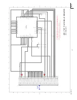
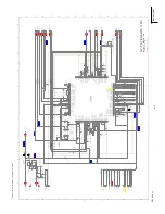
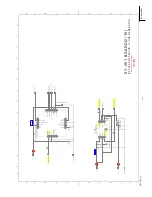
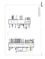
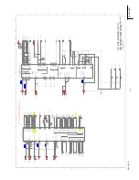
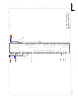
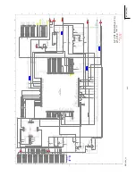
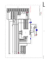
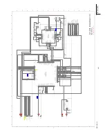
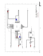
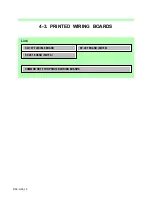
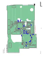
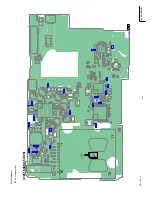
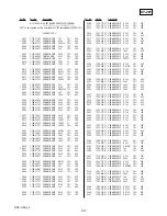
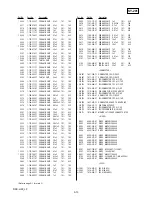
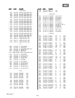
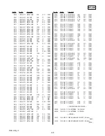
4-3. PRINTED WIRING BOARDS
4-3. PRINTED WIRING BOARDS
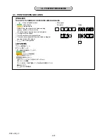
•
: Uses unleaded solder.
•
: Circuit board
: Flexible board
Pattern from the side which enables seeing.
: pattern of the rear side
(The other layers’ patterns are not indicated)
• Through hole is omitted.
• Circled numbers refer to waveforms.
• There are a few cases that the part printed on diagram
isn’t mounted in this model.
•
C
: panel designation
• Chip parts.
Transistor
Diode
(JAPANESE)
ǿȒțǰॴସǶÀǰ
ÞǿȒțǰॴǶÀǰß
ª
«ฑѦಢஎLJߦƌƛŹƳƎ§
ª
«ռನ
«ǽȔǕǟǾȓౡ৲ನ
گƛŹǀศƣǹǧÀț§
«຺ƣǹǧÀț
Î੮ƣǹǧÀțƠƙŹƛƤࠤƊǁƛŹƳƐLjÏ
ªǡȓÀȃÀȓƤंໄ§
ªǿȒțǰॴƠƤ¨ේƜߦƌƛŹƟŹശഌƁ֗ޜƊǁƛŹǀ
त݉ƁŷƿƳƎ§
ª
C
Ƥǹǵȓࠤบआ§
(ENGLISH)
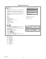
THIS NOTE IS COMMON FOR PRINTED WIRING BOARDS
2
1
3
2
1
3
2
1
3
3
4
5
2
1
1
2
3
6
5
4
E
B
C
3
1
5
2
4
6
1
2
3
6
5
4
3
1
5
2
4
6
1
2
3
5
4
4
3
1
2
3
1 2
4
5
5
3 4
1
2
1
4
2
3
4
6
2
5
3
1
1
2
4
3
1
4
2
3

