C905
1222-9526 rev. 1
FUNCTIONAL OVERVIEW
FU
N
C
T
IO
N
A
L O
V
E
R
V
IE
W
FU
N
C
T
IO
N
A
L O
V
E
R
V
IE
W
Technical Description
FUNCTIONAL OVERVIEW
FU
N
C
T
IO
N
A
L O
V
E
R
V
IE
W
FUNCTIONAL OVERVIEW
FU
N
C
T
IO
N
A
L O
V
E
R
V
IE
W
Bluetooth and FM Radio
The Bluetooth/FM Radio circuit combines Bluetooth and FM tuner functionality into one.
Bluetooth
The Bluetooth implementation is compliant with Bluetooth specification 2.1 + EDR.
The Bluetooth
TM
transceiver has frequency channels with 1 MHz separation from 2402 to
2480 MHz. The same band is used for both transmission and reception. This gives 79
frequency channels.
Receiver
The Bluetooth section implements a low-IF receiver for Bluetooth modulated input
signals. The radio signal is taken from a balanced RF input and amplified by an LNA. The
mixers are driven by two quadrature LO signals, which are locally generated from a VCO
signal running at twice the frequency. The I and Q mixer output signals are band pass
filtered by a poly-phase filter for channel filtering and image rejection. The output of the
band pass filter is amplified by a VGA to the optimal input range for the A/D converter.
Further channel filtering is done in the digital part. The digital part demodulates the
GFSK,
π
/4-DQPSK or 8-DPSK coded bit stream by evaluating the phase information.
RSSI data is extracted. Overall automatic gain amplification in the receive path is
controlled digitally. The RC time constants for the analog filters are automatically
calibrated on chip.
Transmitter
The transmitter uses the serial transmit data from the Bluetooth Controller. The
transmitter modulator converts this data into GFSK,
π
/4-DQPSK or 8-DPSK modulated I
and Q digital signals for respectively 1, 2 and 3 Mbps transmission speed. These signals
are then converted to analog signals that are low pass filtered before up-conversion. The
carrier frequency drift is limited by a closed loop PLL.
FM Radio
FM Receiver
The receiver uses a digital low-IF architecture. The receive (RX) section integrates a low
noise amplifier (LNA) supporting the worldwide FM broadcast band (76 to 108 MHz). An
automatic gain control (AGC) circuit controls the gain of the LNA to optimize sensitivity
and rejection of strong interferers. An image-reject mixer down converts the RF signal to
low-IF. The quadrature mixer output is amplified, filtered and digitized with high
resolution analog-to-digital converters (ADCs). This advanced architecture allows the
use of digital signal processing (DSP) to perform channel selection, FM demodulation
and stereo audio processing.
Tuning
The receiver uses frequency synthesizer technology including a completely integrated
VCO. The frequency synthesizer generates the quadrature local oscillator signal used to
downconvert the RF input to a low intermediate frequency. The VCO frequency is locked
to the reference clock and adjusted with an automatic frequency control (AFC) servo
loop during reception. The tuning frequency is defined as: Freq (MHz) = Spacing (kHz) ×
C Bottom of Band (MHz)
External Connectors
External units are connected to the transceiver by means of a 12-pin connector on the
bottom of the phone.
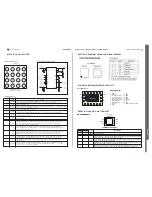
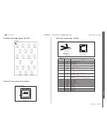
System connector pin input/output overview:
Clocks
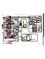
Clock Distribution
The clocking for the access and application subsystems is separated. This means that
the subsystems can wake up or go to sleep mode independently. The access subsystem
is clocked by the 26 MHz Voltage Controlled Crystal Oscillator (VCXO) located in the
GSM/EDGE circuit. When the access subsystem has a job to do, the Master Clock (MCLK)
signal is requested from the RF part. Most other clocks needed within the access
subsystem are generated from the MCLK. Some minor parts like sleep timer and cable
detect use the 32 kHz real-time clock. The 32 kHz real-time clock clocks the application
subsystem, and all other internal clocks needed within the application subsystem are
generated from this clock. However, when audio is transferred between the application
and the access subsystems, the MCLK is used.
Master Clock
(26 MHz)
The 26.00 MHz VCXO-based MCLK is distributed as a square wave signal from the
GSM/EDGE circuit. In order to have full control over the load on the MCLK, only the
access side of the digital baseband controller is allowed to request the MCLK. However,
by indirect means also the application side CPU can issue the request. A VCXO-based
square wave is also distributed to the WCDMA circuit, but is turned on only upon a
command from the digital baseband controller.
Real-time Clock
(32. 768 KHz)
A 32.768 kHz crystal oscillator provides a low frequency clock whenever the platform
has power. This clock is used to keep the Real-Time Clock (RTC) block functioning, so
that the platform can keep track of the time and date. The low frequency clock is
generated in the analog baseband controller and distributed to the digital baseband
controller, and if necessary to external devices like Bluetooth, FM radio and A-GPS.
SEMC Troubleshooting Manual
96
(124)


