background image

C905

1222-9526 rev. 1

TROUBLESHOOTING

  Display Illumination Problems 

TROU

B

L

E

S

H

O

OTIN

G

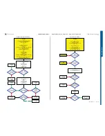
- Opto Sensor Problems

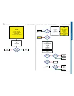
START

Step 1:

Flash the Phone with EMMA SUCR SW

If successful claim SW Flash

If not go to step 2.

Step 2:

Load ITP SW into the Phone

Use TRS Fixture

Connect:

PBA Key Flex Flip, Slider FPC Assy and Display

to the PBA

Connect: VBATT and DCIO/SEPI

Use Fault Trace SW and go to:

MMI

Misc

Init Screen Testing

Led and Backlight

Activate:

Display Backlight

If Display Backlight is working on the TRS Fixture

then Replace

Display, PBA Key Flex Flip or Slider FPC Assy

If not then continue with the

Display ilumination Problems TRS guide

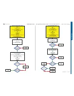
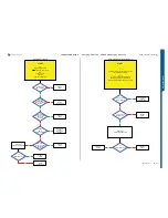
1:

Ues Fault trace SW and go to:

MMI

Misc

Init Screen Testing

Led and Backlight

Deactivate:

Display Backlight

2:

Disconnect Slider FPC Assy from the PBA

3.7V - 3.8V DC 

at MP 51 (TP4200)

3.7V - 3.8V DC

at MP 119

(V4201_Anode)

No

Replace

V4201

Yes

Replace

L4200

No

Fault trace SW

MMI

Misc

Init Screen Testing

Led and Backlight

Activate:

Display Backlight

Yes

17V - 20V DC at

MP 51 (TP4200)

More than

4 Volt DC 

Pk-Pk Pulses

at MP 117

(V4200_Pin 3)

No

Yes

Replace

V4200

SL 5 Replace

 N2000

SL 4 Escalate

No

0 Volt DC at

MP 52 (TP4201)

Yes

Replace

X4200

Yes

Replace

V4203

No

Is the

Display illumination

Problem solved

No

Claim Component

V4203

Yes

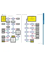
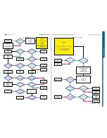
Display Illumination Problems

START

Step 1:

Replace PBA Key Flex Flip

and retest the Phone

If successful claim PBA Key Flex Flip

if not go to step 2.

Step 2:

Replace Slider FPC Assy

and retest the Phone

If successful claim Slider FPC Assy

if not continue with the

Opto Sensor Problems TRS guide

Is the

Display

Illumination (LEDs)

Ok

Go to

Dispaly illumination

Problems TRS guide

No

Can you see

any picture on

Display

Yes

Go to

Display Problems

TRS guide

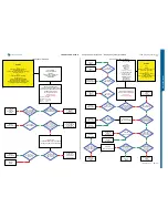
No

Use TRS Fixture

Connect: VBATT and DCIO/SEPI

Yes

1.8 Volt DC at

 MP 73 (R2217

OPTO_EN)

Shortly after phone

Power On

SL 5 Replace

N2000

SL 4 Escalate

No

Yes

3 Volt

Pk-Pk Pulses at

MP 59 (TP2203

VOPTO30) Shortly after

phone Power On

No

Replace

N2201

Replace

X4200

Yes

Is the

Opto Sensor Problem

solved

Claim Component

X4200

No

Yes

SL 5 Replace

N2000

SL 4 Escalate

Opto Sensor Problems

SEMC Troubleshooting Manual

11

 (124)

Содержание Cyber-shot C905

Страница 1: ...C905 1222 9526 rev 1 Troubleshooting Manual APPENDIX COMPONENT OVERVIEW FUNCTIONAL OVERVIEW ABOUT ABOUT TROUBLESHOOTING MEASUREMENT POINTS C905 SEMC Troubleshooting Manual 1 124 ...

Страница 2: ...blems 21 USB VBUS Charging Problems 21 SIM Problems 22 Memory Stick Problems 22 Primary Secondary Mic Problems 23 Ear Speaker Problems 23 Loudspeaker Problems 24 Handsfree PHF Problems 24 FM Radio Problems 25 FM Radio Antenna Problems 25 Bluetooth Problems 26 WLAN Problems 26 GSM Problems 27 WCDMA I II and V Problems 27 WCDMA VIII Problems 28 A GPS Problems 28 Accelerometer Problems 29 Vibrator Pr...

Страница 3: ... RepairToolsCatalogue pdf Instrument Settings Voltage 3 8 Volt Limiter 2 0 A Note Maximal cable length between the Power Supply Channel 1 VBATT and the dummy battery cannot be more than 1 meter The cable must be able to handle at least 16A Power Supply Channel 2 DCIO SEPI Agilent 6632B or similar Location CSPN Repair Instructions Mechanical Tool Catalogue RepairToolsCatalogue pdf Instrument Settin...

Страница 4: ...onyericsson com Drivers DSS SEPI SEMUTS SE Communication Interface SEPI BOX Location CSPN Repair Instructions Mechanical Tool Catalogue RepairToolsCatalogue pdf Part number LTN 214 1484 See Picture 3 Picture 3 Cables USB Computer Cable Location CSPN Repair Instructions Mechanical Tool Catalogue Re See Picture 4 Picture 4 DSU 60 USB Cable Location CSPN Repair Instructions Mechanical Tool Catalogue ...

Страница 5: ... below Step 1 Step 2 Step 3 and Step 4 Step 1 Take the CST 75 battery charger and cut of the charger according to Picture 7 Picture 7 Note The Cable length must be exactly 1 3 meters Step 2 Connect the CST 75 charger Red or White wire to the Plus Output and the Black wire to the Minus GND Output at backside of the Power Supply Channel 2 DCIO SEPI according to Picture 8 Picture 8 Step 3 Cut off ins...

Страница 6: ...nd a BNC plug at the other Manufacturer PMK Germany Location http www elfa se en or other supplier Part number 46 310 40 Note This is the ELFA part number Step 2 Cut the Red Lab Plug connector according to Picture 15 Picture 15 Step 3 Use any Hands Free PHF Cable and cut it according to Picture 16 Picture 16 Note Cable length should be at least 40 cm Step 4 Only use the Wire that is connected to P...

Страница 7: ...M Card See Picture 19 Picture 19 Test SIM GSM UMTS One Test SIM GSM UMTS is needed to perform Current Consumption Test see Picture 20 Location CSPN Repair Instructions Mechanical Tool Catalogue RepairToolsCatalogue pdf Note To buy a Test SIM GSM UMTS please contact your supplier of test equipment Picture 20 Sony Memory Stick M2 Any functional Memory Stick Micro M2 Card See Picture 21 Picture 21 SM...

Страница 8: ...ssful Flash the phone with correct CDA software Yes Flash the phone with correct CDA software Press C Connect USB from PC Run SEMC BOOT if necessary Run SUCR SW Is Phone Flash OK Power On Off Problems START Step 1 Perform System Connector Protection Test If successful go to step 2 Step 2 Load ITP SW into the Phone Go to USB VBUS Charging Problems Does the Phone Indicate charging on the display Yes...

Страница 9: ...p 2 Connect Key Flex Assy and Slider FPC Assy to the PBA Connect VBATT Only Step 3 Use EMMA SW Press the C key and Connect USB Cable from the PC to the PBA Flash the Phone with ITP SW Yes Is the ITP SW Flash Successful SL 5 Replace N2020 SL 4 Escalate Yes Go to USB and Software Flash Problems TRS guide No No Go to Dead Phone Problems part 2 SL 5 Replace N2000 SL 4 Escalate SL 5 Replace N2000 SL 4 ...

Страница 10: ...uide No Is the picture too dark or too light Yes Go to Opto Sensor Problems TRS guide No Disconnect VBATT and DCIO SEPI and Remove PBA from the TRS Fixture Use Digital Multimeter instrument DMM and perform Z4200 Z4201 and Z4202 Display Filter Test 1 and 2 NOTE Be very careful when you re cutting the Shield Can Fence to avoid component damage Yes START Step 1 Flash the Phone with EMMA SUCR SW If su...

Страница 11: ... Backlight Yes 17V 20V DC at MP 51 TP4200 More than 4 Volt DC Pk Pk Pulses at MP 117 V4200_Pin 3 No Yes Replace V4200 SL 5 Replace N2000 SL 4 Escalate No 0 Volt DC at MP 52 TP4201 Yes Replace X4200 Yes Replace V4203 No Is the Display illumination Problem solved No Claim Component V4203 Yes Display Illumination Problems START Step 1 Replace PBA Key Flex Flip and retest the Phone If successful claim...

Страница 12: ... on Numeric Key Foil If successful then Replace Numeric Key Foil If not go to step 3 Step 3 Use TRS Fixture Connect Numeric Key Foil to the PBA Connect VBATT and DCIO SEPI and continue with the Numeric Keypad and Camera Snap Button Problems TRS guide Is the Problem with both Numeric and Navigation Keypads Replace X2410 or X2411 No Yes 1 8 Volt DC at MP 96 S2453_Pin A and MP 94 S2454_Pin A Go to Vo...

Страница 13: ...e S2453 Volume Up Button Yes 0 Volt DC at MP S2453_Pin A and MP S2453_Pin B No Yes Replace S2453 No No No SL 5 Replace N2010 SL 4 Escalate Are MP 96 S2453_Pin A and MP 97 S2453_Pin B short circuit to the PBA GND Shield Can Fence SL 5 Replace R2473 or N2010 SL 4 Escalate Yes Are MP 96 S2453_Pin A and MP 97 S2453_Pin B still short circuit to the PBA GND Shield Can Fence Remove the S2453 Volume Up Bu...

Страница 14: ...ton Yes Is the MP 82 S2415_Pin A and MP 84 S2415_Pin B still Short circuit to GND Shield Can Fence SL 5 Replace V2475 or V2471 SL 4 Escalate Yes Replace S2415 No No SL 5 Replace V2482 SL 4 Escalate Camera Play and Mode REC Button Problems 3 8 Volt DC at MP 160 C2473 SL 5 Replace N2000 SL 4 Escalate No Replace X2410 Yes Connect VBATT and DCIO SEPI Restart the Fault Trace SW and go to MMI Misc Init ...

Страница 15: ...0 SL 4 Escalate No Yes 5 Volt DC at MP 56 TP4400 No Replace N4400 Yes 1 7V 3V DC at MP 78 R4403 MP 77 R4404 MP 75 R4405 and MP 79 R4406 No Yes Navigation Keypad LED Problems 1 4V 1 5V DC at MP 93 TP4401 when Auto Focus LED is Activated No Yes Replace N4400 5 Volt DC at MP 56 TP4400 when Auto Focus LED is Activated Yes No Is the Problem solved SL 5 Replace N2010 SL 4 Escalate No Replace X4400 Yes C...

Страница 16: ...MP 56 TP4400 Yes Replace N4400 Connect VBATT and DCIO SEPI Restart the Fault Trace SW and go to MMI Misc Init Screen Testing Led and Backlight Activate Tally LED START Load ITP SW into the Phone Use TRS Fixture Connect Flash Complete to the PBA Connect VBATT and DCIO SEPI Use Fault Trace SW and go to MMI Misc Init Screen Testing Led and Backlight Activate Tally LED If Tally LED is working on the T...

Страница 17: ...onnect VBATT and DCIO SEPI Restart the Fault Trace SW and go to MMI Misc Init Screen Testing Led and Backlight Activate Camera LED No Replace X4200 Yes 0 Volt DC at MP 92 C4215 and MP 86 C4217 when Camera LED is Activated 0 Volt DC at MP 89 C4218 when Camera LED is Activated SL 5 Replace N2000 SL 4 Escalate Yes SL 5 Replace V4208 SL 4 Escalate No Is the Camera Navigation LED Problem solved SL 5 Re...

Страница 18: ...O SEPI Use Fault Trace SW Fault Trace SW MMI Misc Init Screen Testing Led and Backlight Activate Xenon Flash Test Yes Disconnect Flash Complete 1 8V 2V DC at MP 149 R4304 No 1 8 Volt DC at MP 87 R4303 Replace N2410 No SL 5 Replace N4300 SL 4 Escalate Yes Yes Replace X4400 Is the Xenon Flash Problem solved SL 4 Replace N2410 SL 5 Replace N2010 No Claim Component X4400 Yes Is MP 133 X4410 connected ...

Страница 19: ...hip Problems START Step 1 Replace Camera 8MP and retest the Phone If successful claim Camera 8MP If not go to step 2 Step 2 Use Dummy Battery connected to the Power Supply Channel 1 VBATT Load ITP SW into the Phone Connect DCIO SEPI Use Fault Trace SW MMI Misc Init Screen Testing Activate Camera Test No Yes Is the Multimedia Combo Chip Problems TRS guide done Go to Multimedia Combo Chip Problems T...

Страница 20: ...amage Step 1 Flash the Phone with EMMA SUCR SW If successful claim SW Flash If not go to step 2 Step 2 Load ITP SW into the Phone Use TRS Fixture Connect PBA Key Flex Flip Slider FPC Assy and Display to the PBA Connect VBATT and DCIO SEPI Use Fault Trace SW and go to MMI Misc Init Screen Testing Display Pattern Activate TV Test Pattern No Is the MP X2405_Pin 7 Short circuit to the PBA GND Shield C...

Страница 21: ...SL 5 Replace N2000 Yes Is MP 113 V2412_Cathode Short circuit to PBA GND Shield Can Fence No Replace V2412 Yes Disconnect VBATT and DCIO SEPI No Is L2449 Max 1 Ohm Replace X2405 Yes SL 5 Replace L2449 SL 4 Escalate No No Charging Problems START Step 1 Perform System Connector Protection Test If successful go to step 2 Step 2 Use Phone with Normal SW SSW Use TRS Fixture and connect VBATT Connect USB...

Страница 22: ...19 Yes No 1MHz and 1 8 Volt Pk Pk at MP 107 ST2410 Flash the Phone with EMMA SUCR SW Is C2419 Short circuit SL 5 Replace C2419 SL 4 Escalate Yes SL 5 Replace N2000 SL 4 Escalate No Yes 1MHz and 1 8V 2 2V Pk Pk at MP 34 SP2410 No SL 5 Replace N2010 SL 4 Escalate No Replace X2402 1 8 Volt DC at MP 106 C2413 No SL 5 Replace N2000 SL 4 Escalate Yes Disconnect VBATT and DCIO SEPI Yes SL 4 Replace X2402...

Страница 23: ...r and retest the Phone If successful claim Ear Speaker If not then go to step 2 Step 2 Replace PBA Key Flex Flip If successful claim PBA Key Flex Flip If not then go to step 3 Step 3 Replace Slider FPC Assy If successful claim Slider FPC Assy If not then go to step 4 Step 4 Load ITP SW into the Phone Use TRS Fixture Connect VBATT and DCIO SEPI Use Fault Trace SW Use Hands Free PHF and continue wit...

Страница 24: ...GPIO Manager Application GPIO_Low GPIO_17 Set GPIO_17 to Low 2 Audio and FM Radio Audio Loop Test Audio Input AUX1 Loop Mode Analog Audio Output AUX Earphone Apply Audio Loop START Step 1 Perform System Connector Protection Test If successful go to step 2 Step 2 Load ITP SW into the Phone Use TRS Fixture Connect VBATT and DCIO SEPI Use Fault Trace SW Remove the DCIO SEPI cabel and Insert Hands Fre...

Страница 25: ...at MP 120 R3149 Yes SL 5 Replace N2010 SL 4 Escalate No More than 40 mV AC Pk PK 1 KHz signal at MP 123 R3151 Yes SL 5 Replace N3103 SL 4 Escalate No Signal Generator Instrument Settings Change Amplitude Level to 800 μV Go to FM Radio Antenna Problems TRS guide Yes Is the any of C3145 or C3146 Short circuit No SL 5 Replace C3145 or C3146 SL 4 Escalate Yes 1 8 Volt DC at MP 25 R3302 FM_INT No SL 5 ...

Страница 26: ...lace W1300 SL 4 Escalate Yes 2 7 Volt DC at MP 26 ST1302 VBT27 No SL 4 Replace N1300 SL 5 Replace N2000 No 26 MHz Signal At MP 22 ST2106 BT_CLK Yes No SL 4 Replace N1300 SL 5 Replace N2100 Replace N1300 SL 5 Replace N2010 SL 4 Escalate Yes Bluetooth Problems START NOTE This TRS guide is NOT valid for C905c Phones Step 1 Flash the Phone with EMMA SUCR SW and retest the Phone If successful claim SW ...

Страница 27: ...e GSM Network Problem solved Claim Component N1200 Yes SL 5 Replace N2010 or N2000 SL 4 Escalate No Go to SERP Calibration GSM Network Problems Replace N1210 No Replace N1200 Is the GSM Network Ok Go to GSM Network Problems TRS guide No Fault Trace SW TX and RX WCDMA Radio Settings Select Band BAND I Fast select channels Set Low Channel Ch LOW Modes Max Pwr 23dBm START NOTE This TRS guide is NOT v...

Страница 28: ...es SL 5 Replace L1200 SL 4 Escalate No Is the WCDMA TX Problem solved Go to SERP Calibration WCDMA BAND VIII Network Problems START Step 1 Got to Service Tests Menu and perform the GPS Test If successful Flash the Phone with EMMA SUCR SW if not go to step 2 Step 2 Replace PBA Key Flex Flip and retest the Phone If successful claim PBA Key Flex Flip if not go to step 3 Step 3 Replace Slider FPC Assy...

Страница 29: ... information are changing in the info box Flash the Phone with EMMA SUCR SW Replace N2411 No Is the Accelerometer Problem solved Claim Component N2411 Yes SL 5 Replace N2010 SL 4 Escalate No Yes Accelerometer Problems START Step 1 Load ITP SW into the Phone Step 2 Use TRS Fixture Connect VBATT and DCIO SEPI Use Fault Trace SW and go to MMI Misc Init Screen Testing Activate Vibrator Test 2 7V 3 5V ...

Страница 30: ...he Test Passed Flash the Phone with EMMA SUCR SW Yes SL 4 Replace C2214 SL 5 Replace N2000 No Real Time Clock Problems START Step 1 Replace Numeric Key Foli and retest the Phone If successful claim Numeric Key Foil If not go to step 2 Step 2 Replace Cover Rear Assembly and retest the Phone If successful claim Cover Rear Assembly If not go to step 3 Step 3 Continue with the Slide Sensor Problems TR...

Страница 31: ... N2420 if lower or higher R2446 if higher 12 0L 75K 0L V2412 if lower V2202 if lower C2440 if lower C2441 if lower Current Consumption Test Step 1 Insert a Local SIM Card and use the phone with the Normal SW SSW Use Dummy Battery connected to Power Supply Channel 1 VBATT Instrument settings Voltage 3 8 Volt Limiter 3A Note Dummy Battery The resistance between GND and BDATA should be approximately ...

Страница 32: ...annels Ch LOW Modes Max Pwr 23dBm Limits WCDMA BAND I Transmitter current 550mA Tolerance 25 Max TX Power WCDMA BAND II Note Valid only for C905a Fault Trace SW settings TX and RX WCDMA Radio Settings Select Band BAND I Fast Select Channels Ch LOW Modes Max Pwr 23dBm Limits WCDMA BAND I Transmitter current 470mA Tolerance 20 Max TX Power WCDMA BAND V Note Valid only for C905a Fault Trace SW settin...

Страница 33: ...ith the Normal SW SSW Dummy Battery connected to Power Supply Channel 1 VBATT Note The Dummy Battery should have approximately 27 KOhm resistance between GND and BDATA Power Supply Channel 1 VBATT Instrument settings Voltage from 3 0 Volt to 4 2 Volt according to VBATT row in the Reference Table Limiter 2A Power Supply Channel 2 DCIO SEPI Instrument settings Voltage 5V Limiter 2A Test instructions...

Страница 34: ...ge 3 8V Limiter 2A Power supply Channel 2 DCIO SEPI Voltage 5V Limiter 2A Fault Trace SW go to General Asic Revisions Read All Reference Table ASIC Part number Description Return value hex N2010 1208 3871 CPU Kajsa 0xE8 N2000 1202 0639 Power Management Vera 0xC8 Bluetooth Firmware Revision Ox5 0x3 Chip ID 0x0 0x0 0x0 0x0 N1300 1200 6182 Will always return 0 on STLC because Chip ID is not supported...

Страница 35: ...SHOOTING Measurement Points Pictures TROUBLESHOOTING MP 2 ST1404 Shortly after the phone is powered on Note This is an example The shape of the signal can be different MP 1 MP 30 C3137 and C3148 SEMC Troubleshooting Manual 35 124 ...

Страница 36: ...C905 1222 9526 rev 1 TROUBLESHOOTING TROUBLESHOOTING Measurement Points Pictures MP 19 ST2108 TV_CLK MP 14 L2405 TV_OUT SEMC Troubleshooting Manual 36 124 ...

Страница 37: ...C905 1222 9526 rev 1 TROUBLESHOOTING TROUBLESHOOTING Measurement Points Pictures MP 22 ST2106 BT_CLK MP 20 ST2109 VIDCC_CLK SEMC Troubleshooting Manual 37 124 ...

Страница 38: ...C905 1222 9526 rev 1 TROUBLESHOOTING TROUBLESHOOTING Measurement Points Pictures MP 27 W1300_Pin 4 MP 24 ST2105 WLAN_CLK SEMC Troubleshooting Manual 38 124 ...

Страница 39: ...C905 1222 9526 rev 1 TROUBLESHOOTING TROUBLESHOOTING Measurement Points Pictures MP 32 ST1403 Shortly after the phone is powered on MP 28 W1300_Pin 3 SEMC Troubleshooting Manual 39 124 ...

Страница 40: ...C905 1222 9526 rev 1 TROUBLESHOOTING TROUBLESHOOTING Measurement Points Pictures MP 37 ST2110 CAMSYSCLK MP 34 SP2410 SEMC Troubleshooting Manual 40 124 ...

Страница 41: ...C905 1222 9526 rev 1 TROUBLESHOOTING TROUBLESHOOTING Measurement Points Pictures MP 47 N1500 MP 38 R2102_MCLK SEMC Troubleshooting Manual 41 124 ...

Страница 42: ...C905 1222 9526 rev 1 TROUBLESHOOTING TROUBLESHOOTING Measurement Points Pictures MP 55 ST2107 AGPS_CLK MP 48 C1502 BT_ANT SEMC Troubleshooting Manual 42 124 ...

Страница 43: ...6 rev 1 TROUBLESHOOTING TROUBLESHOOTING Measurement Points Pictures MP 100 MP 101 L3126 L3125 Note This is an example The shape of the signal can be different MP 59 TP2203 VOPTO30 SEMC Troubleshooting Manual 43 124 ...

Страница 44: ...2 9526 rev 1 TROUBLESHOOTING TROUBLESHOOTING Measurement Points Pictures MP 103 C3146 MP 99 MP 102 C3125 C3124 Note This is an example The shape of the signal can be different SEMC Troubleshooting Manual 44 124 ...

Страница 45: ... 9526 rev 1 TROUBLESHOOTING TROUBLESHOOTING Measurement Points Pictures MP 108 MP 109 L2403 L2404 Note This is an example The shape of the signal can be different MP 107 ST2410 SEMC Troubleshooting Manual 45 124 ...

Страница 46: ...526 rev 1 TROUBLESHOOTING TROUBLESHOOTING Measurement Points Pictures MP 98 MP 121 C3156 C3155 Note This is an example The shape of the signal can be different MP 117 V4200_Pin 3 SEMC Troubleshooting Manual 46 124 ...

Страница 47: ...C905 1222 9526 rev 1 TROUBLESHOOTING TROUBLESHOOTING Measurement Points Pictures MP 123 R3151 1 kHz MP 122 C3145 SEMC Troubleshooting Manual 47 124 ...

Страница 48: ...OUBLESHOOTING TROUBLESHOOTING MP 135 ST2104 RTCCLK MP 123 R3151 Handsfree PHF Problems TRS Guide Note This is an example The shape of the signal can be different Measurement Points Pictures SEMC Troubleshooting Manual 48 124 ...

Страница 49: ...C905 1222 9526 rev 1 TROUBLESHOOTING TROUBLESHOOTING MP 138 C2101 32 kHz MP 136 C2100 32 kHz Measurement Points Pictures SEMC Troubleshooting Manual 49 124 ...

Страница 50: ...C905 1222 9526 rev 1 TROUBLESHOOTING TROUBLESHOOTING WLAN TX Output Power MP Vibrator on TRS Fixture Measurement Points Pictures SEMC Troubleshooting Manual 50 124 ...

Страница 51: ...C905 1222 9526 rev 1 TROUBLESHOOTING TROUBLESHOOTING Blt MaxPwr MOD 1 Blt MacPwr MOD 0 Measurement Points Pictures SEMC Troubleshooting Manual 51 124 ...

Страница 52: ...T1519 R1517 SP1503 V2100 R1518 C1528 R1521 R1519 L1502 C1516 C1515 C1514 C1513 L1501 C1517 C1503 L1500 R1514 C1506 C1509 R1512 N1510 C1507 C1508 R1511 ST1520 L1503 SP2102 R1534 R1533 SP1305 R1532 R3100 C3110 ST3103 SP1303 C2281 ST2231 R4300 S4300 ST2232 SP4201 C2286 C4300 R4301 C2280 ST2108 ST2109 C2346 C2302 ST2421 C2301 C2303 R2475 R5101 C2322 C2344 R2471 ST1403 R5102 ST1404 C2323 ST1407 C2304 S...

Страница 53: ...R1210 R1203 C1214 C1204 ST1201 N1210 C1215 ST2212 C1203 C2203 C1205 C2202 C3167 N3103 E1002 V4200 C2201 C2410 C2421 C2422 R3149 C3145 C3133 R3112 C3127 C3155 C3152 C3136 C3100 C3102 C3126 C3156 C3151 C3124 C3125 C3112 N2000 R2403 C2100 R2402 C2402 C4204 R4202 R4204 R2404 R4201 R4200 C4205 ST2104 C2228 C1201 C4202 ST1200 C4203 ST4203 V4201 V2200 ST2211 ST2214 C2229 C2200 X4202 X2401 R3147 N3101 SP3...

Страница 54: ...AT1 VCAMSA28 VBEAR26 VAUDIO26 OPTOSENSE TESTOUT AGPS_CLK BT_CLKREQn WLAN_CLKREQ Application Sys Performance Application Sys Performance Pages B1 B16 VDDE18 Page T1 Test Page T1 not used T01 TV_RESn I02 B03 AGPS_CLK_EN not used R03 A02 FM_SELECT LED_TALLY I04 B16 VIDCC_RESn BTGPIO10 BTGPIO9 BTGPIO16 BTGPIO11 BTGPIO8 BTGPIO0 B14 B14 CH_DET_DM CH_DET_DP I04 XEFL_FCD WLAN_PDn B10 GPIO_P5 GPIO_P4 GPIO_...

Страница 55: ...NTENNA PWRRSTn RTCCLK I2CDAT1 I2CCLK1 VBAT MICN AUXinR MICP AUXinL VDDE18 PWRRSTn I2CDAT1 I2CCLK1 VAD SPL SPR VAUDIO26 VBEAR26 RTCCLK Audio Digital Page 3 Audio Digital Page 3 FM_ANTENNA FM Radio Page 4 FML FMR I2CCLK1 I2CDAT1 FM_ANTENNA RTCCLK VBAT VDDE18 PWRRSTn Page 4 FM Radio VBEAR26 VAUDIO26 VAD SPR SPL FML FMR MICP AUXinL VBAT MICN AUXinR Page 2 Page 2 Audio Analog 1210 8302 Page A1 5 SEMC T...

Страница 56: ...int SP_ref COO SPR SPL MICN MICP INTMIC INTMICint V_MIC TJATTE3 NCP2990 C1 A1 2 A 3 A C2 C3 B3 B1 B2 N3100 1200 9978 INM INP Bypass SHDN OUTB OUTA VP AUDIO_PA VM_P VM 2 2Kohms R3102 33pF NM C3126 33pF C3165 10uF C3166 100ohms R3150 10uF C3106 2 2Kohms R3147 2 2Kohms R3148 100Kohms R3149 0ohms R3160 ST3100 1 2 1uF C3151 220nF C3131 100ohms R3156 33pF C3157 10uF C3158 4 7Kohms R3106 220nF C3112 220n...

Страница 57: ...00 MMI SCK1 WS1 SDI1 SCK2 WS2 SDI2 SDO1 SDO2 MP202 N4 N3 M4 P4 L2 M2 L3 L1 N2500 1200 1414 MP202_I2SIF PM0_SEN PM0_CLK PM0_SO PM0_SI PM1_SEN PM1_CLK PM1_SO PM1_SI 100Kohms R3204 SP3206 SP3207 SP3214 SP3213 NC 100Kohms NM R3201 100Kohms NM R3202 100Kohms NM R3203 DB3210ADT 7POPHF T24 T22 T23 U15 V22 W24 U23 V23 N2010 1208 3871 KAJSA_BOTTOM_APP I2S_PCM_A_10_24 I2S0CLK PCM0CLK I2S0WS PCM0SYN I2S0DLD ...

Страница 58: ... F7 D4 D6 B3 A4 D9 D8 E9 D7 C9 C5 5 B 8 C A5 A6 A7 D5 C7 C6 C4 B7 B6 B4 A3 B8 BLUETOOTH FM_FM FM_FMIP FM_RFGND FM_RST FM_SENB FM_SCL FM_SDA FM_RTCCLK FM_GPIO1 FM_GPIO2 FM_GPIO3 FM_ROUT FM_LOUT NC NC NC NC NC NC FM_VA FM_VD FM_VIO FM_GND FM_GND FM_GND FM_GND FM_GND FM_GND FM_GND FM_GND FM_RADIO_IO FM_PWR_GND 22nF C3304 100nF C3305 3 3Kohms R3302 220pF C3306 270nH L3300 NC NC NC NC NC NC DB3210ADT 7...

Страница 59: ...MSYSCLK RTCCLK VBT27 VCAML12 VCAMIO18 VCAMAF28 RF_ID PWRRSTn VCAMSD18 MCLKSEC CAMRESn OPTO_EN VBEAR26 AGPS_RSTn CHARGE_LED WLAN_VO33 WLAN_LDO18A WLAN_LDO30 OPTOSENSE WLAN_SCLK STEPUP50 LED_KEYPAD OPTOTEMP VOPTO30 WLAN_CLKREQ AGPS_CLK WLAN_CLK WLAN_VO18 BT_CLKREQn LED_CAM1 LED_KEYPAD LED_CAM1 VAUDIO26 VIDCC_SDR_EN DCIO VIDCC_L1_EN SERVICEn STEPUP50 RTCCLK TESTOUT CAM_LDO_EN VCAMSD_EN CAMRESn SPL FM...

Страница 60: ...n WLAN_CLKREQ VIDCC_CLKREQn VDDE18 MCLK VIDCC_CLKREQn ONSWAn SERVICEn BT_CLK CAMSYSCLK BTRESn MCLKREQ RTCCLK DCON USB_HS_CLK PWRRSTn MCLKSEC AGPS_RSTn VIDCC_CLK MEMRESn VDDE18 System Memories Page 4 AGPS_CLK WLAN_CLK BT_CLKREQn WLAN_CLKREQ BT_CLKREQn WLAN_CLKREQ AGPS_CLK WLAN_CLK AGPS_RSTn PWRRSTn DCON VDDE18 SERVICEn MCLK MCLKREQ MEMRESn BTRESn CAMSYSCLK MCLKSEC VIDCC_CLK USB_HS_CLK ONSWAn BT_CLK...

Страница 61: ...LK 3 N2410 GPIO_P2_BIDIR MAX7327 1200 1951 4 GPIO_P3_BIDIR WLAN_CLK 22ohms R2122 22ohms R2123 1 2 ST2100 BT_CLKREQn WLAN_CLKREQ ST2101 2 1 100Kohms R2104 SP2103 Leadfree 1000 0391 V2101 S1D13771 1200 0362 N2700 H7 CLKI S1D13771_CLOCK 1 2 ST2102 1 2 ST2103 SN74LVC2G241YZPR 1204 8667 N2102 2 A 1 D C1 B2 D2 C2 A1 B1 VCC 2OE 1Y 2A GND 2Y 1A 1OE 100Kohms R2116 DB3210ADT 7POPHF 1208 3871 N2010 K12 APPLI...

Страница 62: ... SH_D06 SH_D05 SH_D04 SH_D03 SH_D02 SH_D01 SH_D00 SH_A15 SH_SDBS1 SH_A14 SH_SDBS01 SH_A13 SH_SDBS0 SH_A12 SH_A11 SH_A10 SH_A09 SH_A08 SH_A07 SH_A06 SH_A05 SH_A04 SH_A03 SH_A02 SH_A01 KAJSA_BOTTOM_SH_EMIF_A_8_24 DB3210ADT 7POPHF C12 C13 J12 C14 C15 D16 B15 C16 B17 C17 B18 C18 C19 B20 C20 C21 C22 C23 D21 D23 D22 E23 C24 D24 C25 E24 D25 D13 J11 E12 J10 C10 E11 D7 E14 E13 J14 J15 E15 D15 E16 D17 E17 D...

Страница 63: ...itSDRAMx16 APPLICATIONMEMORYIF EMIF2 1205 5912_POP KAL00900MX AJ55 Y15 T20 U21 U20 V21 V20 W21 Y18 AA19 Y17 AA18 Y16 AA17 D1 E1 R21 M21 T21 N21 B7 A6 B6 A5 B5 B4 A4 A3 C1 F2 F1 G2 H1 J2 J1 K2 D2 P20 E2 R20 N2020 KAL00900MX AJ55_MCP_POP_SDRAM_EMIF1 SDRAM_128_A0 SDRAM_128_A1 SDRAM_128_A2 SDRAM_128_A3 SDRAM_128_A4 SDRAM_128_A5 SDRAM_128_A6 SDRAM_128_A7 SDRAM_128_A8 SDRAM_128_A9 SDRAM_128_A10 SDRAM_12...

Страница 64: ... VBEAR26 VCAML12 VCAMIO18 VAUDIO26 VCAMSA28 VBT27 CHARGE_LED VCAMAF28 VCAMSD18 VIDCC_SDR_EN VIDCC_L1_EN VCAMSD_EN OPTO_EN WLAN_VO33 WLAN_LDO18A WLAN_LDO30 WLAN_SCLK VOPTO30 WLAN_CLKREQ WLAN_VO18 PWRRSTn WLAN_VO33 WLAN_VO18 WLAN_LDO18A WLAN_LDO30 VBAT WLAN_CLKREQ WLAN_SCLK Power WLAN Page 10 VCORE12 VANA25 VMEM18 VDDE18 Page 9 Power Asics VCORE18 VIDCC_L1_EN OPTO_EN VCAML12 VBAT VCAMIO18 VCAMAF28 V...

Страница 65: ...VDD_IO REF TEST IO LEVELS Ericsson AB 3100 POWER TEST VREF IREF SPARE1 SPARE2 VDIG VBEAR26 VBT27 FDMA1027P 1200 0145 V2202 1 2 7 6 S G D D FDMA1027P 1200 0145 V2202 4 5 8 3 G S D D VCORE18 CHARGE_LED 2 1 ST2213 Leadfree 1000 0087 V2201 SP2200 ST2211 1 2 ST2212 1 2 16V 100nF NM C2221 100nF C2227 16V 47pF C2225 100nF C2223 22pF C2202 3 3pF C2203 4 7uF C2206 2 2uF C2209 1uF C2208 1uF C2213 10uF C2217...

Страница 66: ... 4 1 2 1000 8623 CE OUT GND IN 2 2uF C2283 2 2uF C2284 2 2uF C2285 2 2uF C2286 100Kohms R2213 100Kohms R2214 CAM_LDO_EN VCAMSD_EN 100Kohms R2215 ST2226 1 2 OPTO_EN 100Kohms R2217 2 2uF C2289 2 2uF C2288 3V R1115Z301D 2 1 4 3 N2201 1000 8623 CE OUT GND IN TP2203 VOPTO30 VCORE18 100Kohms R2221 100Kohms R2223 2 2uF C2248 NC NC NC NC NC NC NC NC NC NC NC NC 2 2uF C2251 2 2uF C2250 ST2230 2 1 ST2231 1 ...

Страница 67: ...AE18 AE20 AE19 1208 3871 PLL_FILTER KAJSA_BOTTOM_PLL PLL_PG_416_FILTVDD PLL_PG_416_VCONT PLL_26_FILTVDD PLL_26_VCONT KAJSA_BOTTOM_PLL_A_15_24 DB3210ADT 7POPHF N2010 AE15 AD16 AB12 AB10 AD17 AD18 AE13 AE12 AD19 AB7 AC18 AC19 R2 AB15 AE14 AE16 AC12 AC11 AC17 AB14 1208 3871 VDD_ANALOG VDDIO KAJSA_BOTTOM_2 5V_POWER GNDE_ANA VSSCOMMON VSSGPAD GNDAD VSSDA VSS_AD2 VSS_AD1 VSSCO_PLL_3_4 VSSCO_PLL_1_2 VDD_...

Страница 68: ...LAN_LDO18A WLAN_LDO30 100nF C2373 2 2uH L2313 VBAT BLM18PG121SN1 L2310 1000 0118 4 7uH L2311 MAX7327 N2410 12 1200 1951 GPIO_O10_OUTPUT 100Kohms R2313 WLAN_SCLK 88PW886 1203 2790 2 8 4 1 18 15 20 6 16 2 19 3 9 12 17 5 14 7 10 13 11 N2300 MARVELL_88PW886_2 SVIN PVIN PVIN SLEEPn PDn SDI GND SW3 VO3 PGND SW1 VO1 PGND SW2 FB2 PGND VO2 VL2X VL2Y VL3 NC WLAN_CLKREQ WLAN_VO18 NC ST2310 2 1 ST2311 2 1 ST2...

Страница 69: ...R VAUDIO26 VBAT DCON VDDE18 USB_HS_CLK RF_ID VIDCC_CLK RTCCLK VIDCC_CLKREQn VIDCC_SDR_EN VIDCC_L1_EN CAM_LDO_EN VCAMSD_EN CAMRESn MICN AUXinR MICP AUXinL FM_ANTENNA SERVICEn DCIO VBUS VMC18 ONSWAn OPTOSENSE STEPUP50 LED_KEYPAD VAUDIO26 OPTOTEMP RF_ID VAD AID_AD Page 12 VBACKUP VDDE18 I2CCLK1 I2CDAT1 TX_ADSTR VDIG OPTOSENSE TESTOUT Page 12 ADC DAC OPTOTEMP VBUS SERVICEn FM_ANTENNA MICP AUXinL DCIO ...

Страница 70: ...hms R2408 3 3Kohms R2405 3 3Kohms R2406 4 7Kohms R2403 1 4 7Kohms R2404 1 4 7Kohms R2402 1 RF_ID 4 7Kohms R2400 VDIG 100nF C2405 100nF C2406 10uF C2404 ST2401 2 1 ST2402 1 2 SP2400 SP2401 MAX7327 N2410 18 24 9 25 22 23 19 20 21 1200 1951 HEATSLUG INT MAX7327_MAIN SCL SDA RST AD0 AD2 GND V 100nF C2403 ST2400 1 2 OPTOTEMP LIS331DL N2411 2 3 10 5 12 13 16 15 11 9 14 1 7 6 4 8 1202 1676 GND_RES GND GN...

Страница 71: ...8 100Kohms R2419 100Kohms R2420 10Kohms R2416 10Kohms R2415 2 2uF C2410 VMC18 1 X2401 2 1200 9764 5 2 3 4 6 7 8 470Kohms R2422 10 11 22 21 20 19 18 17 16 15 14 13 12 9 SIMHOLDER SHIHO 5 6 3 7 2 1 X2402 1202 0528 SIMCONDAT NC GND SIMCONCLK SIMCONRST SIMVCC NC NC NC NC NC SP2411 SP2412 100nF C2421 2 2uF C2422 DB3210ADT 7POPHF N2010 AC23 AD24 AC24 AA22 AB22 AC25 AB24 AA23 1208 3871 MMC SD MSPRO_IF KA...

Страница 72: ...z L2403 100MHz L2402 100MHz L2401 VDDE18 100Kohms R2447 470ohms R2442 VDDE18 100Kohms NM R2440 ST2421 2 1 ST2422 2 1 0ohms R2443 1201 2253 V2413 2 A 1 A 1 8uH L2405 1 5Kohms R2452 1 75ohms R2453 100pF C2444 270pF C2445 560ohms R2451 1 33pF C2446 1201 8440 V2415 1 2 C A 1201 8440 V2416 1 2 C A 100nF C2449 BZX585C15 1000 0272 V2417 1 2 C A 33pF NM C2438 NC NC NC NC NC NC TCM1210 900 2P T 1201 6833 Z...

Страница 73: ...IN4 KEYIN5 KAJSA_BOTTOM_CONNECTIVITY KEYPAD_INTERFACE DB3210ADT 7POPHF N24 N2010 1208 3871 APPLICATION GPIO_04 X2411 1 ESDALC6V1 1BM2 2 1 V2474 1207 3081 A C ESDALC6V1 1BM2 V2477 1 2 1207 3081 A C ESDALC6V1 1BM2 V2475 1 2 1207 3081 A C ESDALC6V1 1BM2 V2476 1 2 1207 3081 A C ESDALC6V1 1BM2 2 1 V2471 1207 3081 A C ESDALC6V1 1BM2 V2472 1 2 1207 3081 A C ESDALC6V1 1BM2 V2473 1 2 1207 3081 A C ESDALC6V...

Страница 74: ...SK SPI1_SI SPI1_SO INT_B SPI0_CSZ SPI0_SK SPI0_SI SPI0_SO MP202_HOSTIF_SPI MP202 N2500 N12 M13 M12 M11 M3 L12 L11 K10 K9 K6 K5 K4 J12 J10 J5 J3 H12 H3 G12 G3 F12 F10 F6 F5 F3 E10 E9 E6 E5 E4 D12 D10 D5 D4 C13 C12 C11 C8 C7 C4 B12 1200 1414 IC IC IC IC IC IC IC IC IC IC IC IC IC IC IC IC IC IC IC IC IC IC IC IC IC IC IC IC IC IC IC IC IC IC IC IC IC IC IC IC IC MP202_IC MP202 N2500 J2 C2 B11 C3 B3 ...

Страница 75: ...50 STEPUP50 LED_BACK LED_CAM1 VBAT VDDE18 VCAMSA28 VCAMAF28 I2CCLK1 CAMSYSCLK I2CDAT1 VDIG VCAML12 VCAMIO18 VCAMSD18 CAM_LDO_EN CAMRESn VOPTO30 CHARGE_LED STEPUP50 OPTOTEMP OPTOSENSE LED_KEYPAD XEFL_SPDA LMU XEFL_SPDA LED_BACK VBAT I2CDAT1 VDDE18 I2CCLK1 XEFL_CHARGE_CTRL XEFL_TRIG STEPUP50 Page 4 LMU LED_CAM1 Display LED_BACK VOPTO30 OPTOTEMP CHARGE_LED OPTOSENSE VBAT VDDE18 VDIG LED_CAM1 LED_KEYP...

Страница 76: ...2 X4200 12 100 pin 1 6 11 13 16 14 15 17 19 21 18 20 22 24 9 27 29 1 3 TP4201 10 25 26 31 46 47 53 76 OPTOTEMP OPTOSENSE 100nF C4229 80 VOPTO30 CHARGE_LED LED_KEYPAD 59 75 82 83 91 95 100 78 99 23 NC MEA1608LC220T001 1000 7455 1 2 3 4 5 6 7 8 9 10 Z4200 EMI FILTER O1 2 I1 1 I2 1 I3 1 I4 1 O2 2 O3 2 O4 2 GND_1 GND_2 MEA1608LC220T001 1000 7455 1 2 3 4 5 6 7 8 9 10 Z4201 EMI FILTER O1 2 I1 1 I2 1 I3 ...

Страница 77: ...CLK1 I2CDAT1 CAM_LDO_EN SN74LVC2G66YZPR 1200 0333 S4300 D1 A2 A1 B1 B2 D2 C2 C1 NM 1A 1B 2C GND 1C 2A 2B VCC 0ohms R4301 0ohms R4300 100nF NM C4300 VDDE18 100nF C4301 100nF C4303 CAMRESn 100nF C4320 XEFL_TRIG 1200 1733 A2 30 pin X4300 B14 B13 B12 A3 B10 B9 B8 B7 B6 B5 A15 B3 B2 A1 B1 B15 B11 A4 A5 A6 A7 A8 A9 A10 A11 A12 A13 A14 B4 Z1 Z2 Z3 Z4 MAX7327 1200 1951 N2410 13 GPIO_O11_OUTPUT RYT326 1000...

Страница 78: ...4414 NM 0ohms R4406 33pF C4415 NM Z1 Z2 B8 B1 A10 A8 A7 1 2 24 pin X4400 A1 1201 5197 B7 B6 B5 B4 B3 B2 A2 A3 A4 A5 A6 A9 BLM15EG121SN1 L4401 1Kohms R4409 XEFL_TRIG 4 7uH L4400 A11 XEFL_CHARGE_CTRL 100Kohms R4411 Z3 Z4 A12 B9 XEFL_SPDA 10uF C4416 1 2 ST4400 0ohms R4413 SP4400 SP4401 SP4402 SP4403 SP4404 STEPUP50 52 54 48 50 LED_BACK MAX8830 N4400 D4 D3 C3 A2 A4 1 D 3 B B2 B1 C1 B4 C2 A1 C4 D2 1200...

Страница 79: ...POWDET WTX_QA WRX_QA WTX_QB WRX_QB WTX_IA WRX_IA WTX_IB WDETON WPA2_EN WPA1_EN WPA0_EN DCLK_DATSTR AMP_LSB_FREQ_LSB IDATA_FREQ_MSB QDATA_AMP_MSB ANTSW3 ANTSW2 ANTSW1 ANTSW0 RADDAT TESTOUT RADCLK MCLK RADSTR MCLKSEC MCLKREQ WRX_IB OPTO_EN GSM UMTS Page 2 XEFL_SPDA 100Kohms R1103 100Kohms R1101 100Kohms R1102 WLAN_CLKREQ WLAN_SCLK WLAN_LDO30 ACC_SPI_DI WLAN_CONFIRMn WLAN_CLK VDIG ACC_SPI_DO ACC_SPI_...

Страница 80: ... A4 A2 N1210 MAX8805 REFBP AGND REFIN PGND LDO2 PA_EN EN2 LX IN2 HP IN1B IN1A LDO1 EN1 PAB PAA 220nF C1213 100nF C1214 100nF C1215 1uF C1216 NM 2 2uF C1217 2 2uF C1218 100Kohms R1209 100Kohms R1210 2 2uF C1219 NM 68pF NM C1220 2 8V RP102K281D TR 1204 5903 1 4 2 6 5 7 3 N1211 VDD_2 CE GND VOUT_1 SLUG VDD_1 VOUT_2 RP102K 0ohms NM R1211 22pF C1221 NM TIGER_I_VIII_MODULE 1210 9905 N1200 D8 E9 C9 D9 F9...

Страница 81: ...RSRV_D STLC2593 1200 9840 L2 D3 E1 E2 E4 N7 E6 M6 J9 N3 N5 G8 G1 D1 D2 E3 F1 F2 F3 F4 G3 G4 H3 H4 H6 H7 H8 K8 L8 J2 K2 L1 H1 N1300 BT_VSS_RF BTPOWER GND BT_VSS_RF BT_VSS_RF BT_VSS_RF BT_VSS_DIG BT_VSS_DIG BT_VSS_DIG BT_VSS_DIG BT_VSS_DIG BT_VSS_ANA BT_VSS_ANA BT_VSS_ANA BT_VSS_ANA BT_VSS_ANA BT_VSS_ANA BT_VSS_ANA BT_VSS_ANA BT_VSS_ANA BT_VSS_ANA BT_VSS_ANA BT_VSS_ANA BT_VDD_CLD BT_VIO_E BT_VIO_D B...

Страница 82: ... 100Kohms R1403 100Kohms R1402 NM 100Kohms R1401 10Kohms NM R1406 ST1407 1 2 1 2 ST1406 X4200 100 pin 89 4 6 2 1204 5252 85 97 93 96 98 84 86 88 92 94 90 100Kohms R1404 ST1405 2 1 MAX7327 1200 1951 N2410 8 GPIO_O7_OUTPUT MAX7327 1200 1951 2 N2410 GPIO_O1_OUTPUT 87 0ohms R1407 0ohms R1408 120pF C1400 NM 220nH L1400 NM DB3210ADT 7POPHF 1208 3871 N2010 W5 ACCESS GPIO_17 N2010 V5 ACCESS GPIO_10 W3 ACC...

Страница 83: ...SPI_DO ACC_SPI_CLK NC NC NC NC NC NC NC NC NC NC NC NC NC 10pF C1502 WLAN_CLKREQ WLAN_SCLK CRS5001 4202E X1500 2 1 6 5 4 3 1203 9688 GND GND GND GND C_TERM R_TERM WLAN_VO18 SP1500 SP1501 SP1502 100Kohms R1525 0ohms R1526 NM MAX7327 11 N2410 1200 1951 GPIO_O9_OUTPUT SP1503 W_FL R SMT 1_48 X1530 4 3 2 1 1001 0637 100Kohms R1527 0ohms R1532 0ohms R1533 NM 0ohms R1534 NM 1nF C1503 SP1504 2 7nH NM L150...

Страница 84: ...1 ETM_PSTAT0 ETM_TPKT7 ETM_TPKT6 ETM_TPKT5 ETM_TPKT4 ETM_TPKT3 ETM_TPKT2 ETM_TPKT1 ETM_TPKT0 ETM_TSYNC ETM_TCLK KAJSA_BOTTOM_ETM_A_17_24 DB3210ADT 7POPHF R5 A1 A2 A3 B1 C1 AD1 AE1 AF1 AF2 AF3 AF24 AF25 AF26 AE26 AD26 A26 B26 C26 A25 A24 N2010 1208 3871 KAJSA_BOTTOM_NOT_USED KAJSA_BOTTOM_UNUSED EFUSE_HV5 UNUSED UNUSED UNUSED UNUSED UNUSED UNUSED UNUSED UNUSED UNUSED UNUSED UNUSED UNUSED UNUSED UNUS...

Страница 85: ...8 B2 C2304 1000 0048 B2 C2305 1000 0048 C2 C2306 1000 0048 C2 C2307 1000 0048 C2 C2308 1000 0048 C2 C2309 1000 0048 C2 C2310 1000 0048 C3 C2311 1000 0048 C3 C2312 1000 0048 C3 C2313 1000 0048 C3 C2314 1000 0048 C2 C2320 1000 0051 C2 C2321 1000 0048 C3 C2322 1000 0048 B2 C2323 1000 0048 B2 C2324 1000 0048 C2 C2325 1000 0048 C2 C2326 1000 0048 C2 C2327 1000 0048 C2 C2328 1000 0048 C2 C2329 1000 0048...

Страница 86: ...00 0068 C2 C2290 1000 6900 C2 C2292 1000 0048 C2 C2402 1000 0048 B4 C2410 1000 6901 B3 C2412 1000 0048 B4 C2413 1000 0338 B4 C2414 1000 0051 B4 C2419 1000 0045 D3 C2420 1000 0051 D3 C2421 1000 0048 B3 C2422 1000 6901 B3 C2430 1000 0048 B4 C2440 1000 0076 B4 C2441 1000 0057 B4 C2442 1000 0045 B4 C2443 1000 0045 B4 C2447 1000 6838 B4 C2448 1000 6838 B4 C2449 1000 0048 B4 C3100 1000 6900 B4 C3112 100...

Страница 87: ...ght Red eye reduction PictBridge printing Image stabilizer Video stabilizer Picture blogging Video blogging Video recording Music Media player Bluetooth stereo A2DP Album art Music tones MP3 AAC PlayNow TrackID Internet Access NetFront Web browser Web feeds Communication Video calling Speaker phone Polyphonic ringtones Vibrating alert Messaging Email Exchange ActiveSync Text messaging SMS Picture ...

Страница 88: ...crophone interface Stereo line input Earphone driver Earpiece driver 8 Ω speaker driver Stereo line output The analog baseband controller is controlled by an I2C interface It also comprises the main power management circuits equipped with a number of converters and regulators for generating the required supply voltages The analog baseband controller supports the following features Lithium battery ...

Страница 89: ...C905 1222 9526 rev 1 FUNCTIONAL OVERVIEW FUNCTIONAL OVERVIEW Technical Description Functional Blocks of the Analog Baseband Controller Connection Diagram SEMC Troubleshooting Manual 89 124 ...

Страница 90: ...device The pass device is automatically turned off when an external source is detected on DCIO or when the watchdog termination block times out The watchdog termination block must be active when the external switch is enabled both in normal charging mode and in the low resistive path mode The watchdog is set through the serial interface and if it has not been set again before timeout the watchdog ...

Страница 91: ...plifier The earphone amplifiers BEARP and BEARN are mainly intended to be differentially configured and drive a low impedance dynamic transducer earpiece but they can also be single ended configured The BEARP and BEARN amplifiers can be powered down by the I2C The amplifiers can exhibit high impedance to 1 4V or low impedance to ground when powered down Fifty one gains are available for BEARP and ...

Страница 92: ... communication with an external SDRAM The Shared EMIF is shared between the Access subsystem and the Application subsystem Access Subsystem Application Subsystem The Application subsystem contains functionality related to functions such as MMI graphics audio and memory media The control CPU is an ARM926 with three external memory interfaces one shared with the Access subsystem and two dedicated fo...

Страница 93: ...or low band 850 900 MHz and one for high band 1800 1900 MHz The EDGE GSM GPRS power amplifier output is filtered by the low pass filter in the Front End and then connected to the antenna through a switch In receive mode the EDGE GSM GPRS signal from the antenna passes through the switch to one of the four receive SAW filters The SAW filter provides receive band selectivity In GSM GRPS EDGE systems...

Страница 94: ...se locked Loop PLL has two information inputs the divider ratio in the feedback path and a direct path to the VCO The phase locked loop generates the radio frequency carrier including the phase modulation information at the desired channel frequency WCDMA Transmitter Part The WCDMA transmitter architecture is an on frequency linear direct up conversion IQ modulator The in phase and quadrature phas...

Страница 95: ...TX Frequency Range 1710 2 MHZ 1784 8 MHZ Channel Range TX 512 885 Power Level Min 15 Max 0 PCS 1900 TX Frequency Range 1850 2 MHZ 1909 8 MHZ Channel Range TX 512 810 Power Level Min 15 Max 0 RX Frequency and Channel Range GSM 850 RX Frequency Range 869 2 MHZ 893 8 MHZ Channel Range RX 128 251 GSM 900 Frequency Range 935 2 MHZ 959 8 MHZ Channel Range RX 1 124 EGSM 900 RX Frequency Range 925 2 MHZ 9...

Страница 96: ...ADCs This advanced architecture allows the use of digital signal processing DSP to perform channel selection FM demodulation and stereo audio processing Tuning The receiver uses frequency synthesizer technology including a completely integrated VCO The frequency synthesizer generates the quadrature local oscillator signal used to downconvert the RF input to a low intermediate frequency The VCO fre...

Страница 97: ...g the A GPS module with a highly accurate timing reference The A GPS is able to accurately synchronize its GPS time to this reference pulse A GPIO used as an enable POWERON signal to the GPS module A GPIO used for power control for the GPS module A GPS Block Diagram WLAN Wi Fi This WLAN module is based on the new Marvell 88W8686 chipset WLAN module is designed to support IEEE 802 11a or 802 11g pa...

Страница 98: ...raffic if it is a BT high request All WLAN traffic should have priority before any BT traffic that is categorized as BT low requests WLAN Driver sends status events to BT Driver to inform about WLAN startup and shutdown WLAN association and disassociation The current WLAN channel in use In the cases of WLAN startup and shutdown the BT Logical Driver configures the BT Device to request the antenna ...

Страница 99: ... AM DAC RFCtrl1 RFCtrl2 RFCtrl1 RFCtrl2 GSM EDGE HB GSM EDGE LB WCDMA LB WCDMA HB WCDMA HB GSM EDGE LB GSM EDGE LB GSM EDGE HB GSM EDGE HB WRxIA WRxIB WRxQB WRxQA EDataB EDataA EDataC EDataStr RF 3300 WCDMA RX other functions unused MCLKsec CLKREQ MCLK XO XOp TestOut GSM EDGE PA Ant Sw VAPC PA PA GSM850 900 Input DCS PCS Input ESD VccWPA En Bias VccWPA En Bias VccWPA En Bias WRX1_In WRX1_Ip WRX1_Q...

Страница 100: ...A VBAT_C VBUS VBUS Charger VBAT_H VBAT_K VBAT_L DVDD AVDD RF Subsystem Buck 1 2V 1 05 600mA VCCPA VIO_X2 VIO_X1 VDD18A VDD18_LDO VDD30 Back up capacitor 4 7k PoP 12 20 VCCDA VDDIO VDDIO_PLL VDDCO_PLL VCCAD VCCGPAD VDDCO VDDAD D VDDQ F VDD 10 6 Control Bluetooth Subsystem WLAN Subsystem VBAT VACT VDIG VANA DAC1 DAC2 REF VCONTROL VBAT VDDA_AF VDDANA 2 5 V 1 2 V BOOST W LED driver VBAT_M LED5n VCC1 V...

Страница 101: ...C905 1222 9526 rev 1 FUNCTIONAL OVERVIEW Block Diagram Clocking Concept FUNCTIONAL OVERVIEW SEMC Troubleshooting Manual 101 124 ...

Страница 102: ... 1974 105 B N2213 Step Down Converter 500mA 1208 4678 105 F N2300 ASIC Power Management 1203 2790 106 F N2410 IC IF 3 5x3 5x0 8 thin QFN 1200 1951 106 F N2411 ASIC Accelerometer 1202 1676 106 F N2420 IC IF ISP1508 ES3 3 5 3 5 0 8 1200 1694 107 Side Pos Description Part Number Comments Page F N2421 IC ESD Prot UDFN 6 2x2 mm 1200 6309 107 B N2422 ASIC Baseband 1201 4120 107 F N2500 Companion chip MP...

Страница 103: ...0 13 mm in mm 0 5 0 05 0 5 0 05 1 0 0 05 0 25 0 1 Resistance element becomes dominant at high frequencies Dimension Equivalent Circuit L2401 04 Filter 0 0 Hz 0402 REG70618 20 0 4 0 2 1 6 0 15 0 8 0 15 0 8 0 15 in mm L2406 Filter 1209 2182 0 116 0 003 2 95 0 076 Dash number 0 116 0 003 2 95 0 076 0 130 3 30 0 040 1 02 0 025 0 64 0 045 1 16 0 020 0 51 0 130 3 30 0 035 0 004 0 9 0 1 Recommended Land ...

Страница 104: ... a 1μF ceramic capacitor as close as possible to LDO1 and AGND LDO1 is internally pulled down through a 1k Ω resistor when this regulator is disabled D2 EN1 LDO1 Enable Input Connect to IN2 or logic high for normal operation Connect to AGND or logic low for shutdown mode D3 D4 PAB PAA PA Connection for Bypass Mode Internally connected to IN1_ using the internal bypass MOSFET during bypass mode PA_...

Страница 105: ...PIO General Purpose Input Output Pins BT_GPIO_0 G9 General purpose I O Configuration Pins BT_CONFIG_1 L7 N O C _ T B BT_CONFIG_3 N6 RF Signals BT_RFP K1 BT_RFN J1 Power Supply BT_HVA BT_HVD N7 BT_VIO_A M6 BT_VIO_C N3 BT_VIO_D N5 BT_VIO_E G8 BT_VIO_B J9 BT_VDD_CLD E6 Bluetooth Section Name I O 4 Input PD Input PD Input PU 6 Input PU 6 Input PD 6 Input PD 6 I O 4 Input PU 6 Input PU 6 function Input...

Страница 106: ...er supply for I O pins 2 NC Not Connected 3 NC Not Connected 4 SCL SPC I2 C Serial Clock SCL SPI Serial Port Clock SPC 5 GND 0V supply 6 SDA SDI SDO I2C Serial Data SDA SPI Serial Data Input SDI 3 wire Interface Serial Data Output SDO 7 SDO SPI Serial Data Output I2 C less significant bit of the device address 8 CS SPI enable I2C SPI mode selection 1 I 2C mode 0 SPI enabled 9 INT 2 Inertial interr...

Страница 107: ...requency depends on status on CFG1 and CFG2 pins XTAL2 F6 AI O Crystal output If crystal is not in use leave this pin open CHIP_SEL C3 I Active HIGH chip select input When this pin is none active ULPI pins will be in 3 state and the chip 1 Symbol names ending with underscore N for example NAME_N indicate active low signals 2 I input O output I O Digital Input Output OD Open Drain Output AI O Analo...

Страница 108: ...ns marked as NC are not used and must be left unconnected Pins marked as Reserved must be left unconnected unless otherwise specified S1D13771 W CSP 64 pin Pinout Top View 1 2 3 4 5 6 7 8 A NC GPIO3 TE COREVDD D C MD2 MD4 NC A B TESTEN VSS GPIO_INT CS IOVDD VSS MD5 SCANEN B C Reserved GPIO2 RESET VSS WE IOVDD MD6 MD7 C D VSS GPIO1 IOVDD CS SEL RD MD3 IOVDD COREVDD D E COREVDD GPIO0 VSS LCDCS MD0 R...

Страница 109: ...ts the Flash Mode The flash duration and FLED flash current are set in I 2 C registers The Flash Mode ends when either FLEN transitions back to logic 0 or after the flash duration timer expires in case FLEN gets stuck high C3 SCL I 2 C Clock Input Data is read on the rising edge of SCL D3 SDA I 2 C Data Input Data is read on the rising edge of SCL D4 VDD Logic Input Supply Voltage Connect VDD to t...

Страница 110: ... 2 0 05 0 8 0 05 CATHODE MARK 0 6 0 1 0 12 0 05 JEDEC SOD 523 0 3 0 05 B SOT 563 CASE 463A PLASTIC 1 6 Q1 1 2 3 4 5 6 Q2 BC847CDXV6T1 MARKING DIAGRAMS 1x M 1x Device Code x G or M M Date Code Pb Free Package Note Microdot may be in either location 1 X1210 X1211 X3102 X3103 Conn Leaf Spring 1200 2144 X1200 X1500 RF Probe Contact 6 Pin 1203 9688 V4203 Trans Array 1200 0320 V2470 V4201 Schottky Barri...

Страница 111: ...PENDIX APPENDIX Components X1540 X2201 X2401 X2402 X1540 Clip BT Antenna 1211 1063 X2201 Battery Leaf Connector 1201 0774 X2401 Memory Card Reader RNK87147 3 X2402 SIM Card Reader 1202 0528 SEMC Troubleshooting Manual 111 124 ...

Страница 112: ... X4200 X4300 X4311 15 X4400 X2410 BtB Receptable 24pin 1208 3264 X4200 100 pin FPC Connector 1204 5252 X4311 12 13 14 15 Ground Spring Finger 1 pin 1204 9353 X4300 Conn BtB 30 pin 1200 1733 X4400 Conn BtB 24 pin 1201 5197 SEMC Troubleshooting Manual 112 124 ...

Страница 113: ...410 Pogopin Plug 1pin 1208 0925 Equivalent circuit 4 2 1 3 0 6 0 07 0 55 0 1 1 25 0 07 1 2 4 3 Dimensions in mm 1 0 0 07 0 25 0 1 0 05 0 3 0 1 e e Ch1 Ch2 Ch3 Ch4 Z4200 Z4201 Z4202 LC Filter REV50148 1 Z2400 Filter 100 Mhz K1210 1201 6833 SEMC Troubleshooting Manual 113 124 ...

Страница 114: ...PESD15VS1UL A C V1111 1 2 1201 0746 PESD15VS1UL A C B1000 4 1 5 3 2 1207 0781 MRUS61C SLUG GND VCC OUT NC A B A1 B1 C D S1003 3 1200 2072 EVPAHAA6A 1 2 OUT1 IN1 IN2 OUT2 GND OUT3 L1000 MMZ1005A152ET L1001 L1002 MMZ1005A152ET L1003 L1004 MMZ1005A152ET L1005 2 1 V1112 1201 0746 PESD15VS1UL A C A11 A12 B11 B12 NC NC 1211 7646 V1100 C A 2 1200 8900 V1103 C A 1211 7646 V1101 C A 1201 0746 2 1 NM V1113 ...

Страница 115: ...r the Tx and Rx tab The main radio functions of the mobile phone presented in this tab are x GSM radio part x WCDMA radio part x Bluetooth radio part In the GSM and the WCDMA radio control part the following radio functions can be controlled Transmitter TX and Receiver RX In the Bluetooth radio control part only the Transmitter TX function is supported Base Band Controls Note Some parts of Base Ba...

Страница 116: ...according to picture 2 Cut off isolation material from inside of the charger plug according to picture 3 Picture 1 Picture 2 Picture 3 Power Supply Channel 2 DCIO SEPI Cable Connection Setup Note The Power Supply Channel 1 VBATT must allow reverse current Note The maximal cable length between the Power Supply Channel 1 VBATT and the dummy battery must not exceed 1m The cable must have a capacity f...

Страница 117: ...SM band Available options are GSM 850 Ch 128 251 GSM 900 Ch 1 124 EGSM 900 Ch 975 1023 DCS 1800 Ch 512 885 and PCS 1900 Ch 512 810 2 Use default value or select desired channel 3 Use default value or select desired power level Note Any GSM band not used by the Mobile Phone will be unavailable in the GSM Radio Settings GSM RSSI measurements This measurement is only possible to perform when RX Switc...

Страница 118: ...ne the VCXO to MCLK frequency by calibrating the DAC that sets the VCXO control voltage It is also used to verify the VCXO tuning range When transmission is in Switched TX mode you are allowed to calibrate the VCXO oscillator controlling the DAC value on the AFC pin 1 Switch the GSM tester to GSM900 Ch1 2 Read the stored VCXO value from the GDFS by clicking the Read from GD button 3 Start transmit...

Страница 119: ...cy Range used in the Troubleshooting Software is from 87 50 MHz to 108 00 MHz Examples of different FM Radio Test setups in the Troubleshooting Software Picture 11 Picture 12 K850 Project FM Radio Setup K800 Project FM Radio Setup Logic Tab Logic Functions Note Some of the Logic functions may not be possible to implement for all products due to limitations in the ITP Software Note There are some d...

Страница 120: ...ort is not supported by the ITP SW SIM Card Control This section controls the SIM interface in the phone SIM VCC Voltage for the SIM Card will be activated SIM RESET SIM DATA and SIM CLOCK Activate the Reset Data and Clock signals for the SIM Card SIM Com Test Checks the communication with the SIM Card The test result Passed or Failed will be displayed in the info box Note A SIM card must be inser...

Страница 121: ...ut more information about which components are included in this test go to the ASIC Revision Test document included in the product specific Troubleshooting Manual Self Test This function runs available self tests on the Phone Troubleshooting Software Documentation Fault Trace SW Error Messages 1 timeout when reading Check the following items Connection between Power Supply Channel 2 DCIO and SEPI ...

Страница 122: ... needed according to picture 5 Picture 5 Open the Top part of the TRS Fixture according to picture 6 Picture 6 Place the PBA by using the Guide Pin mounted inside the TRS Fixture according to picture 7 Picture 7 Connect the Numeric Key Foil with the Keyboard directly to the PBA if needed according to picture 8 Picture 8 Connect the Flash Complete directly to the PBA if needed according to picture ...

Страница 123: ...nd 18 Picture 17 Picture 18 Check that the Ear Speaker is connected properly to the PBA Key Flex Flip see picture 19 Picture 19 Connect Power Supply Channel 1 VBATT Black and Red Lab Plugs to the TRS Fixture according to picture 20 Picture 20 Connect the Power Supply Channel 2 Cable DCIO SEPI according to picture 21 Picture 21 Secure the DCIO SEPI Cable by using the locking screw according to pict...

Страница 124: ...27 Picture 27 Step 2 Connect the Hands Free PHF connector to he Phone system connector X2405 according to picture 28 Picture 28 Please see picture 29 for the final Customized FM Radio Cable connection setup with the TRS Fixture Picture 29 The PIN marked with the GND text on the Top part of the TRS Fixture can be used as MP TRS Fixture GND or grounding for the oscilloscope probe see picture 30 Pict...

Отзывы: