


S i 5 3 x x - R M
98
Rev. 0.52
7.11.3. C1B, C2B (Si5319, Si5324, Si5325, Si5326, Si5327, Si5374, Si5375)
A LOS condition causes the associated
LOS1_INT
or
LOS2_INT
read only register bit to be set. A LOS condition
on CKIN_1 will also be reflected onto C1B if
CK1_BAD_PIN
= 1. Likewise, a LOS condition on CKIN_2 will also be
reflected onto C2B if
CK2_BAD_PIN
= 1.
A FOS condition causes the associated
FOS1_INT
or
FOS2_INT
read only register bit to be set. FOS monitoring is
enabled or disabled using the
FOS_EN
bit. If FOS is enabled (
FOS_EN
= 1) and CK1_BAD_PIN = 1, a FOS
condition will also be reflected onto its associated output pin, C1B or C2B. If FOS is disabled (
FOS_EN
= 0), the
FOS1_INT
and
FOS2_INT
register bits do not affect the C1B and C2B alarm outputs, respectively.
Once an LOS or FOS alarm is asserted on one of the input clocks, it is held high until the input clock is validated
over a designated time period. The validation time is programmable via the
VALTIME
[1:0] register bits as shown in
Table 48 on page 95. If another error condition on the same input clock is detected during the validation time then
the alarm remains asserted and the validation time starts over.
[Si5326]: Note that hitless switching between input clocks applies only when the input clock validation time
VALTIME
[1:0] = 01 or higher.
7.11.4. LOS (Si5319, Si5375)
A LOS condition causes the LOS_INT read only register bit to be set. This LOS condition will also be reflected onto
the INT_CB pin.
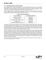
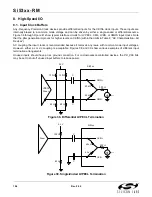
7.11.5. C1B, C2B, C3B, ALRMOUT (Si5367, Si5368, Si5369 [CK_CONFIG_REG = 0])
The generation of alarms on the C1B, C2B, C3B, and ALRMOUT outputs is a function of the input clock
configuration, and the frequency offset alarm enable as shown in Table 52. The
LOSn_INT
and
FOSn_INT
signals
are the raw outputs of the alarm monitors. These appear directly in the device status registers. Sticky versions of
these bits (
LOSn_FLG
,
FOSn_FLG
) drive the output interrupt and can be individually masked. When the device
inputs are configured as four input clocks (
CK_CONFIG
= 0), the ALRMOUT pin reflects the status of the CKIN4
input. The equations below assume that the output alarm is active high; however, the active polarity is selectable
via the
CK_BAD_POL
bit.
Operation of the C1B, C2B, C3B, and ALRMOUT pins is enabled based on setting the
C1B_PIN
,
C2B_PIN
,
C3B_PIN
, and
ALRMOUT_PIN
register bits. Otherwise, the pin will tri-state. Also, if
INT_PIN
= 1, the interrupt
functionality will override the appearance of ALRMOUT at the output even if
ALRMOUT_PIN
= 1.
Once an LOS or FOS alarm is asserted for one of the input clocks, it is held high until the input clock is validated
over a designated time period. The validation time is programmable via the
VALTIME
[1:0] register bits as shown in
Table 48 on page 95. If another error condition on the same input clock is detected during the validation time then
the alarm remains asserted and the validation time starts over.
Note that hitless switching between input clocks applies only when the input clock validation time
VALTIME
[1:0] = 01 or higher.
For details, see "Appendix D—Alarm Structure" on page 144.
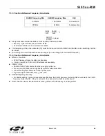
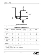
Table 52. Alarm Output Logic Equations (Si5367, Si5368, and Si5369 [CONFIG_REG = 0])
FOS_EN
Alarm Output Equations
0
(Disables FOS)
C1B =
LOS1_INT
C2B =
LOS2_INT
C3B =
LOS3_INT
ALRMOUT =
LOS4_INT
1
C1B =
LOS1_INT
or
FOS1_INT
C2B =
LOS2_INT
or
FOS2_INT
C3B =
LOS3_INT
or
FOS3_INT
ALRMOUT =
LOS4_INT
or
FOS4_INT
Содержание Si5316 Series
Страница 2: ...Si53xx RM 2 Rev 0 52 ...
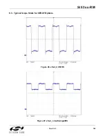
Страница 109: ...Si53xx RM Rev 0 52 109 8 3 Typical Scope Shots for SFOUT Options Figure 46 sfout_2 CMOS Figure 47 sfout_3 lowSwingLVDS ...
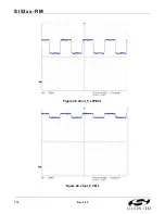
Страница 110: ...Si53xx RM 110 Rev 0 52 Figure 48 sfout_5 LVPECL Figure 49 sfout_6 CML ...
Страница 111: ...Si53xx RM Rev 0 52 111 Figure 50 sfout_7 LVDS ...
Страница 127: ...Si53xx RM Rev 0 52 127 Figure 66 155 52 MHz In 622 08 MHz Out Loop BW 7 Hz Si5324 ...
Страница 128: ...Si53xx RM 128 Rev 0 52 Figure 67 19 44 MHz In 156 25 MHz Out Loop BW 80 Hz ...
Страница 129: ...Si53xx RM Rev 0 52 129 Figure 68 19 44 MHz In 156 25 MHz Out Loop BW 5 Hz Si5324 ...
Страница 130: ...Si53xx RM 130 Rev 0 52 Figure 69 27 MHz In 148 35 MHz Out Light Trace BW 6 Hz Dark Trace BW 110 Hz Si5324 ...
Страница 131: ...Si53xx RM Rev 0 52 131 Figure 70 61 44 MHz In 491 52 MHz Out Loop BW 7 Hz Si5324 ...
Страница 132: ...Si53xx RM 132 Rev 0 52 Figure 71 622 08 MHz In 672 16 MHz Out Loop BW 6 9 kHz ...
Страница 133: ...Si53xx RM Rev 0 52 133 Figure 72 622 08 MHz In 672 16 MHz Out Loop BW 100 Hz ...
Страница 134: ...Si53xx RM 134 Rev 0 52 Figure 73 156 25 MHz In 155 52 MHz Out ...
Страница 139: ...Si53xx RM Rev 0 52 139 Figure 78 86 685 MHz In 173 371 MHz Out ...
Страница 140: ...Si53xx RM 140 Rev 0 52 Figure 79 86 685 MHz In 693 493 MHz Out ...
Страница 142: ...Si53xx RM 142 Rev 0 52 Figure 81 10 MHz In 1 GHz Out ...
Страница 174: ...Si53xx RM 174 Rev 0 52 Figure 99 Si5374 Si5375 DSPLL A ...
Страница 175: ...Si53xx RM Rev 0 52 175 Figure 100 Si5374 Si5375 DSPLL B ...
Страница 176: ...Si53xx RM 176 Rev 0 52 Figure 101 Si5374 Si5375 DSPLL C ...


