


Si53xx-RM
Rev. 0.52
89
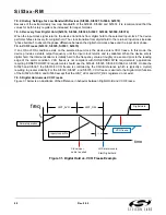
7.7. Output Phase Adjust (Si5326, Si5368)
The device has a highly accurate, digitally controlled device skew capability. For more information on Output Phase
Adjustments, see both DSPLL
sim
and the respective data sheets. Both can be downloaded by going to
www.silabs.com/timing
and clicking on “Documentation” at the bottom of the page.
7.7.1. Coarse Skew Control (Si5326, Si5368)
With the
INCDEC_PIN
register bit set to 0 (pin control off), overall device skew is controlled via the
CLAT
[7:0]
register bits. This skew control has a resolution of 1/f
OSC
, approximately 200 ps, and a range from –25.6 to
25.4 ns. Following a powerup or reset (RST pin or
RST_REG
register bit), the skew will revert to the reset value.
Any further changes made in the skew register will be read and compared to the previously held value. The
difference will be calculated and applied to the clock outputs. All skew changes are made in a glitch-free fashion.
When a phase adjustment is in progress, any new
CLAT
[7:0] values are ignored until the update is complete. The
CLATPROG
register bit is set to 1 during a coarse skew adjustment. The time for an adjustment to complete is
dependent on bandwidth and the delta value in CLAT. To verify a written value into CLAT, the CLAT register should
be read after the register is written. The time that it takes for the effects of a CLAT change to complete is
proportional to the size of the change, at 83 msec for every unit change, assuming the lowest available loop
bandwidth was selected. For example, if CLAT is zero and has the value 100 written to it, the changes will
complete in
100 x 83 msec = 8.3 sec.
If it is necessary to set the high-speed output clock divider N1_HS to divide-by-4 in order to achieve the desired
overall multiplication ratio and output frequency, only phase increments are allowed and negative settings in the
CLAT register or attempts to decrement the phase via writes to the CLAT register will be ignored. Because of this
restriction, when there is a choice between using N1_HS = 4 and another N1_HS value that can produce the
desired multiplication ratio, the other N1_HS value should be selected. This restriction also applies when using the
INC pin.
With the INCDEC_PIN register bit set to 1 (pin control on), the INC and DEC pins function the same as they do for
pin controlled parts. See "6.6. Output Phase Adjust (Si5323, Si5366)" on page 70.
7.7.1.1. Unlimited Coarse Skew Adjustment (Si5326, Si5368)
Using the following procedure, the CLAT register can be used to adjust the device clock output phase to an
arbitrarily large value that is not limited by the size of the CLAT register:
1. Write a phase adjustment value to the CLAT register (Register 16). The DSPLL
sim
configuration software
provides the size of a single step.
2. Wait until
CLATPROGRESS
= 0 (register 130, bit 7), which indicates that the adjustment is complete (Maximum
time for adjustment: 20 seconds for the Si5326 or Si5368).
3. Set
INCDEC_PIN
= 1 (Register 21, bit 7).
4. Write 0 to
CLAT
register (Register 16).
5. Wait until
CLATPROGRESS
= 0.
6. Set
INCDEC_PIN
= 0.
7. Repeat the above process as many times as desired.
Steps 3-6 will clear the
CLAT
register without changing the output phase. This allows for unlimited output clock
phase adjustment using the
CLAT
register and repeating steps 1–3 as many times as needed.
Note:
The INC and DEC pins must stay low during this process.
7.7.2. Fine Skew Control (Si5326, Si5368)
An additional fine adjustment of the overall device skew can be used in conjunction with the INC and DEC pins or
the
CLAT
[7:0] register bits to provide finer resolution output phase adjustments. Fine phase adjustment is available
using the
FLAT
[14:0] bits. The nominal range and resolution of the
FLAT
[14:0] skew adjustment word are:
Range
FLAT
= ±110 ps
Resolution
FLAT
= 9 ps
Содержание Si5316 Series
Страница 2: ...Si53xx RM 2 Rev 0 52 ...
Страница 109: ...Si53xx RM Rev 0 52 109 8 3 Typical Scope Shots for SFOUT Options Figure 46 sfout_2 CMOS Figure 47 sfout_3 lowSwingLVDS ...
Страница 110: ...Si53xx RM 110 Rev 0 52 Figure 48 sfout_5 LVPECL Figure 49 sfout_6 CML ...
Страница 111: ...Si53xx RM Rev 0 52 111 Figure 50 sfout_7 LVDS ...
Страница 127: ...Si53xx RM Rev 0 52 127 Figure 66 155 52 MHz In 622 08 MHz Out Loop BW 7 Hz Si5324 ...
Страница 128: ...Si53xx RM 128 Rev 0 52 Figure 67 19 44 MHz In 156 25 MHz Out Loop BW 80 Hz ...
Страница 129: ...Si53xx RM Rev 0 52 129 Figure 68 19 44 MHz In 156 25 MHz Out Loop BW 5 Hz Si5324 ...
Страница 130: ...Si53xx RM 130 Rev 0 52 Figure 69 27 MHz In 148 35 MHz Out Light Trace BW 6 Hz Dark Trace BW 110 Hz Si5324 ...
Страница 131: ...Si53xx RM Rev 0 52 131 Figure 70 61 44 MHz In 491 52 MHz Out Loop BW 7 Hz Si5324 ...
Страница 132: ...Si53xx RM 132 Rev 0 52 Figure 71 622 08 MHz In 672 16 MHz Out Loop BW 6 9 kHz ...
Страница 133: ...Si53xx RM Rev 0 52 133 Figure 72 622 08 MHz In 672 16 MHz Out Loop BW 100 Hz ...
Страница 134: ...Si53xx RM 134 Rev 0 52 Figure 73 156 25 MHz In 155 52 MHz Out ...
Страница 139: ...Si53xx RM Rev 0 52 139 Figure 78 86 685 MHz In 173 371 MHz Out ...
Страница 140: ...Si53xx RM 140 Rev 0 52 Figure 79 86 685 MHz In 693 493 MHz Out ...
Страница 142: ...Si53xx RM 142 Rev 0 52 Figure 81 10 MHz In 1 GHz Out ...
Страница 174: ...Si53xx RM 174 Rev 0 52 Figure 99 Si5374 Si5375 DSPLL A ...
Страница 175: ...Si53xx RM Rev 0 52 175 Figure 100 Si5374 Si5375 DSPLL B ...
Страница 176: ...Si53xx RM 176 Rev 0 52 Figure 101 Si5374 Si5375 DSPLL C ...


