


Si53xx-RM
Rev. 0.52
95
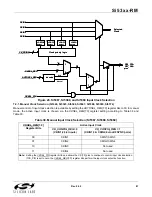
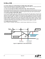
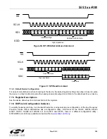
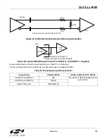
7.10. PLL Bypass Mode (Si5319, Si5324, Si5325, Si5326, Si5327, Si5367, Si5368, Si5369,
Si5374, Si5375)
The device supports a PLL bypass mode in which the selected input clock is fed directly to the output buffers,
bypassing the DSPLL. In PLL bypass mode, the input and output clocks will be at the same frequency. PLL bypass
mode is useful in a laboratory environment to measure system performance with and without the jitter attenuation
provided by the DSPLL. The
BYPASS_REG
bit controls enabling/disabling PLL bypass mode.
Before going into bypass mode, it is recommended that the part enter Digital Hold by setting
DHOLD
. Internally, the
bypass path is implemented with high-speed differential signaling for low jitter. Note that the CMOS output format
does not support bypass mode.
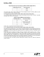
7.11. Alarms (Si5319, Si5324, Si5325, Si5326, Si5327, Si5367, Si5368, Si5369, Si5374,
Si5375)
Summary alarms are available to indicate the overall status of the input signals and frame alignment (Si5368 only).
Alarm outputs stay high until all the alarm conditions for that alarm output are cleared. The Register
VALTIME
controls how long a valid signal is re-applied before an alarm clears. Table 48 shows the available settings. Note
that only for
VALTIME
[1:0] = 00, hitless switching is not possible.
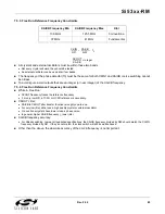
7.11.1. Loss-of-Signal Alarms (Si5319, Si5324, Si5325, Si5326, Si5327, Si5367, Si5368, Si5369, Si5374,
Si5375)
The device has loss-of-signal circuitry that continuously monitors CKINn for missing pulses. The LOS circuitry
generates an internal
LOSn_INT
output signal that is processed with other alarms to generate CnB and
ALARMOUT.
An LOS condition on CKIN1 causes the internal
LOS1_INT
alarm become active. Similarly, an LOS condition on
CKINn causes the
LOSn_INT
alarm become active. Once a
LOSn_INT
alarm is asserted on one of the input
clocks, it remains asserted until that input clock is validated over a designated time period. If another error
condition on the same input clock is detected during the validation time then the alarm remains asserted and the
validation time starts over.
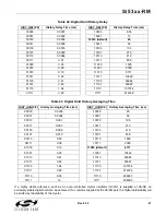
7.11.1.1. Narrowband LOS Algorithms (Si5319, Si5324, Si5326, Si5327, Si5368, Si5369, Si5374, Si5375)
There are three options for LOS: LOS, LOS_A, and no LOS, which are selected using the
LOSn_EN
registers. The
values for the
LOSn_EN
registers are given in Table 49.
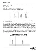
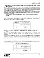
Table 48. Loss-of-Signal Validation Times
VALTIME[1:0]
Clock Validation Time
00
2 ms
(hitless switching not available)
01
100 ms
10
200 ms
11
13 s
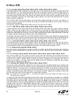
Table 49. Loss-of-Signal Registers
LOSn_EN[1:0]
LOS Selection
00
Disable all LOS monitoring
01
Reserved
10
LOS_A enabled
11
LOS enabled
Содержание Si5316 Series
Страница 2: ...Si53xx RM 2 Rev 0 52 ...
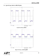
Страница 109: ...Si53xx RM Rev 0 52 109 8 3 Typical Scope Shots for SFOUT Options Figure 46 sfout_2 CMOS Figure 47 sfout_3 lowSwingLVDS ...
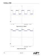
Страница 110: ...Si53xx RM 110 Rev 0 52 Figure 48 sfout_5 LVPECL Figure 49 sfout_6 CML ...
Страница 111: ...Si53xx RM Rev 0 52 111 Figure 50 sfout_7 LVDS ...
Страница 127: ...Si53xx RM Rev 0 52 127 Figure 66 155 52 MHz In 622 08 MHz Out Loop BW 7 Hz Si5324 ...
Страница 128: ...Si53xx RM 128 Rev 0 52 Figure 67 19 44 MHz In 156 25 MHz Out Loop BW 80 Hz ...
Страница 129: ...Si53xx RM Rev 0 52 129 Figure 68 19 44 MHz In 156 25 MHz Out Loop BW 5 Hz Si5324 ...
Страница 130: ...Si53xx RM 130 Rev 0 52 Figure 69 27 MHz In 148 35 MHz Out Light Trace BW 6 Hz Dark Trace BW 110 Hz Si5324 ...
Страница 131: ...Si53xx RM Rev 0 52 131 Figure 70 61 44 MHz In 491 52 MHz Out Loop BW 7 Hz Si5324 ...
Страница 132: ...Si53xx RM 132 Rev 0 52 Figure 71 622 08 MHz In 672 16 MHz Out Loop BW 6 9 kHz ...
Страница 133: ...Si53xx RM Rev 0 52 133 Figure 72 622 08 MHz In 672 16 MHz Out Loop BW 100 Hz ...
Страница 134: ...Si53xx RM 134 Rev 0 52 Figure 73 156 25 MHz In 155 52 MHz Out ...
Страница 139: ...Si53xx RM Rev 0 52 139 Figure 78 86 685 MHz In 173 371 MHz Out ...
Страница 140: ...Si53xx RM 140 Rev 0 52 Figure 79 86 685 MHz In 693 493 MHz Out ...
Страница 142: ...Si53xx RM 142 Rev 0 52 Figure 81 10 MHz In 1 GHz Out ...
Страница 174: ...Si53xx RM 174 Rev 0 52 Figure 99 Si5374 Si5375 DSPLL A ...
Страница 175: ...Si53xx RM Rev 0 52 175 Figure 100 Si5374 Si5375 DSPLL B ...
Страница 176: ...Si53xx RM 176 Rev 0 52 Figure 101 Si5374 Si5375 DSPLL C ...


