


S i 5 3 x x - R M
170
Rev. 0.52
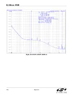
Figure 96. Ground Plane and Reset
RSTL_x Pins
It is highly recommended that the four RSTL_x pins (RSTL_A, RSTL_B, RSTL_C and RSTL_D) be logically
connected to one another so that the four DSPLLs are always either all in reset or are all out of reset. While in
reset, the DSPLLs VCO will continue to run, and, because the VCOs will not be locked to any signal, they will drift
and can be any frequency value within the VCO range. If a drifting VCO happens to have a frequency value that is
close to an operational DSPLLs VCO, there could be crosstalk between the two VCOs. To avoid this issue, Si537x
DSPLLsim initializes the four DSPLLs with default Free Run frequency plans so that the VCO values are apart from
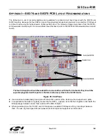
one another. If the four RSTL_x pins are directly connected to one another, the connections should not occur
directly underneath the BGA package. Instead, the connections should occur outside of the package footprint.
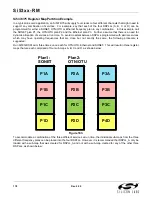
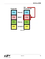
These
four
resistors
force
the
common
RESET
connection
away
from
the
BGA
footprint
Содержание Si5316 Series
Страница 2: ...Si53xx RM 2 Rev 0 52 ...
Страница 109: ...Si53xx RM Rev 0 52 109 8 3 Typical Scope Shots for SFOUT Options Figure 46 sfout_2 CMOS Figure 47 sfout_3 lowSwingLVDS ...
Страница 110: ...Si53xx RM 110 Rev 0 52 Figure 48 sfout_5 LVPECL Figure 49 sfout_6 CML ...
Страница 111: ...Si53xx RM Rev 0 52 111 Figure 50 sfout_7 LVDS ...
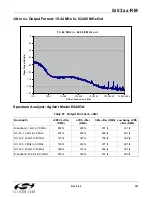
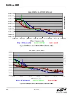
Страница 127: ...Si53xx RM Rev 0 52 127 Figure 66 155 52 MHz In 622 08 MHz Out Loop BW 7 Hz Si5324 ...
Страница 128: ...Si53xx RM 128 Rev 0 52 Figure 67 19 44 MHz In 156 25 MHz Out Loop BW 80 Hz ...
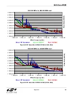
Страница 129: ...Si53xx RM Rev 0 52 129 Figure 68 19 44 MHz In 156 25 MHz Out Loop BW 5 Hz Si5324 ...
Страница 130: ...Si53xx RM 130 Rev 0 52 Figure 69 27 MHz In 148 35 MHz Out Light Trace BW 6 Hz Dark Trace BW 110 Hz Si5324 ...
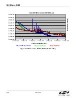
Страница 131: ...Si53xx RM Rev 0 52 131 Figure 70 61 44 MHz In 491 52 MHz Out Loop BW 7 Hz Si5324 ...
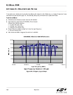
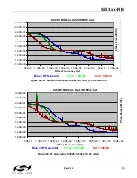
Страница 132: ...Si53xx RM 132 Rev 0 52 Figure 71 622 08 MHz In 672 16 MHz Out Loop BW 6 9 kHz ...
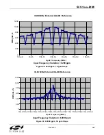
Страница 133: ...Si53xx RM Rev 0 52 133 Figure 72 622 08 MHz In 672 16 MHz Out Loop BW 100 Hz ...
Страница 134: ...Si53xx RM 134 Rev 0 52 Figure 73 156 25 MHz In 155 52 MHz Out ...
Страница 139: ...Si53xx RM Rev 0 52 139 Figure 78 86 685 MHz In 173 371 MHz Out ...
Страница 140: ...Si53xx RM 140 Rev 0 52 Figure 79 86 685 MHz In 693 493 MHz Out ...
Страница 142: ...Si53xx RM 142 Rev 0 52 Figure 81 10 MHz In 1 GHz Out ...
Страница 174: ...Si53xx RM 174 Rev 0 52 Figure 99 Si5374 Si5375 DSPLL A ...
Страница 175: ...Si53xx RM Rev 0 52 175 Figure 100 Si5374 Si5375 DSPLL B ...
Страница 176: ...Si53xx RM 176 Rev 0 52 Figure 101 Si5374 Si5375 DSPLL C ...