


S i 5 3 x x - R M
88
Rev. 0.52
7.6.2. History Settings for Low Bandwidth Devices (Si5324, Si5327, Si5369, Si5374)
Because of the extraordinarily low loop bandwidth of the Si5324, Si5369 and Si5374, it is recommended that the
values for both history registers be increased for longer histories.
7.6.3. Recovery from Digital Hold (Si5319, Si5324, Si5326, Si5327, Si5368, Si5369, Si5374)
When the input clock signal returns, the device transitions from digital hold to the selected input clock. The device
performs hitless recovery from digital hold. The clock transition from digital hold to the returned input clock includes
“phase buildout” to absorb the phase difference between the digital hold clock phase and the input clock phase.
7.6.4. VCO Freeze (Si5319, Si5325, Si5367, Si5375)
If an LOS or FOS condition exists on the selected input clock, the device enters VCO freeze. In this mode, the
device provides a stable output frequency until the input clock returns and is validated. When the device enters
digital hold, the internal oscillator is initially held to the frequency value at roughly one second prior to the leading
edge of the alarm condition. VCO freeze is not compliant with SONET/SDH MTIE requirements; applications
requiring SONET/SDH MTIE requirements should use the Si5324, Si5326, Si5368, Si5369 or Si5374. Unlike the
Si5325 and Si5367, the Si5319’s VCO freeze is controlled by the XA/XB reference (which is typically a crystal)
resulting in greater stability. For the Si5319, Si5327, and Si5375, VCO freeze is similar to the Digital Hold function
of the Si5326, Si5368, and Si5369 except that the
HIST_AVG
and
HIST_DEL
registers do not exist.
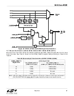
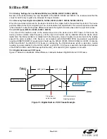
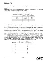
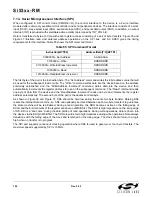
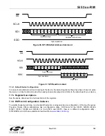
7.6.5. Digital Hold versus VCO Freeze
Figure 31 below is an illustration of the difference in behavior between Digital Hold and VCO Freeze.
Figure 31. Digital Hold vs. VCO Freeze Example
Normal operation
Input clock drifts
f
0
freq
LOS alarm occurs,
Start Digital hold
Digital Hold
VCO freeze
HIST_AVG
HIST_DEL
Clock input
cable is pulled
time
~1 sec
Содержание Si5316 Series
Страница 2: ...Si53xx RM 2 Rev 0 52 ...
Страница 109: ...Si53xx RM Rev 0 52 109 8 3 Typical Scope Shots for SFOUT Options Figure 46 sfout_2 CMOS Figure 47 sfout_3 lowSwingLVDS ...
Страница 110: ...Si53xx RM 110 Rev 0 52 Figure 48 sfout_5 LVPECL Figure 49 sfout_6 CML ...
Страница 111: ...Si53xx RM Rev 0 52 111 Figure 50 sfout_7 LVDS ...
Страница 127: ...Si53xx RM Rev 0 52 127 Figure 66 155 52 MHz In 622 08 MHz Out Loop BW 7 Hz Si5324 ...
Страница 128: ...Si53xx RM 128 Rev 0 52 Figure 67 19 44 MHz In 156 25 MHz Out Loop BW 80 Hz ...
Страница 129: ...Si53xx RM Rev 0 52 129 Figure 68 19 44 MHz In 156 25 MHz Out Loop BW 5 Hz Si5324 ...
Страница 130: ...Si53xx RM 130 Rev 0 52 Figure 69 27 MHz In 148 35 MHz Out Light Trace BW 6 Hz Dark Trace BW 110 Hz Si5324 ...
Страница 131: ...Si53xx RM Rev 0 52 131 Figure 70 61 44 MHz In 491 52 MHz Out Loop BW 7 Hz Si5324 ...
Страница 132: ...Si53xx RM 132 Rev 0 52 Figure 71 622 08 MHz In 672 16 MHz Out Loop BW 6 9 kHz ...
Страница 133: ...Si53xx RM Rev 0 52 133 Figure 72 622 08 MHz In 672 16 MHz Out Loop BW 100 Hz ...
Страница 134: ...Si53xx RM 134 Rev 0 52 Figure 73 156 25 MHz In 155 52 MHz Out ...
Страница 139: ...Si53xx RM Rev 0 52 139 Figure 78 86 685 MHz In 173 371 MHz Out ...
Страница 140: ...Si53xx RM 140 Rev 0 52 Figure 79 86 685 MHz In 693 493 MHz Out ...
Страница 142: ...Si53xx RM 142 Rev 0 52 Figure 81 10 MHz In 1 GHz Out ...
Страница 174: ...Si53xx RM 174 Rev 0 52 Figure 99 Si5374 Si5375 DSPLL A ...
Страница 175: ...Si53xx RM Rev 0 52 175 Figure 100 Si5374 Si5375 DSPLL B ...
Страница 176: ...Si53xx RM 176 Rev 0 52 Figure 101 Si5374 Si5375 DSPLL C ...


