


S i 5 3 x x - R M
70
Rev. 0.52
6.6. Output Phase Adjust (Si5323, Si5366)
Overall device skew (CKINn to CKOUT_n phase delay) is controllable via the INC and DEC input pins. A positive
pulse applied at the INC pin increases the device skew by 1/f
OSC
, one period of the DCO output clock. A pulse on
the DEC pin decreases the skew by the same amount. Since f
OSC
is close to 5 GHz, the resolution of the skew
control is approximately 200 ps. Using the INC and DEC pins, there is no limit to the range of skew adjustment that
can be made. Following a power-up or reset, the skew will revert to the reset value.
The INC pin function is not available for all frequency table selections. DSPLL
sim
reports this whenever it is used
to implement a frequency plan.
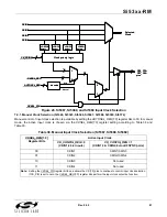
6.6.1. FSYNC Realignment (Si5366)
The FS_ALIGN pin controls the realignment of FS_OUT to the active CKIN3 or CKIN4 input. The currently active
frame sync input is determined by which input clock is currently being used by the PLL. For example, if CKIN1 is
being selected as the PLL input, CKIN3 is the currently-active frame sync input. If neither CKIN3 or CKIN4 are
currently active (digital hold), the realignment request is ignored. The active edge used for realignment is the
CKIN3 or CKIN4 rising edge.
FS_ALIGN operates in Level Sensitive mode (See Figure 19, “Frame Synchronization Timing.”). While FS_ALIGN
is active, each active edge of the currently-active frame sync input (CKIN3 or CKIN4) is used to control the NC5
output divider and therefore the FS_OUT phase. Note that while the realignment control is active, it cannot be
guaranteed that a fixed number of high-frequency clock (CKOUT2) cycles exists between each FS_OUT cycle.
The resolution of the phase realignment is 1 clock cycle of CKOUT2. If the realignment control is not active, the
NC5 divider will continuously divide down its f
CKOUT2
input. This guarantees a fixed number of high-frequency
clock (CKOUT2) cycles between each FS_OUT cycle.
At power-up or any time after the PLL has lost lock and relocked, the device automatically performs a realignment
of FS_OUT using the currently active sync input. After this, as long as the PLL remains in lock and a realignment is
not requested, FS_OUT will include a fixed number of high-speed clock cycles, even if input clock switches are
performed. If many clock switches are performed in phase build-out mode, it is possible that the input sync to
output sync phase relationship will shift due to the accumulated residual phase transients of the phase build-out
circuitry. If the sync alignment error exceeds the threshold in either the positive or negative direction, an alignment
alarm becomes active. If it is then desired to reestablish the desired input-to-output sync phase relationship, a
realignment can be performed. A realignment request may cause FS_OUT to instantaneously shift its output edge
location in order to align with the active input sync phase.
6.6.2. Including FSYNC Inputs in Clock Selection (Si5366)
The frame sync inputs, CKIN3 and CKIN4, are both monitored for loss-of-signal (LOS3_INT and LOS4_INT)
conditions. To include these LOS alarms in the input clock selection algorithm, set FS_SW = 1. The LOS3_INT is
logically ORed with LOS1_INT and LOS4_INT is ORed with LOS2_INT as inputs to the clock selection state
machine. If it is desired not to include these alarms in the clock selection algorithm, set FS_SW = 0. The FOS
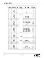
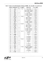
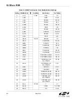
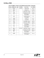
alarms for CKIN3 and CKIN4 are ignored. See Table 33 on page 73.
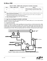
6.6.3. FS_OUT Polarity and Pulse Width Control (Si5366)
Additional output controls are available for FS_OUT. FS_OUT is active high, and the pulse width is equal to one
period of the CKOUT2 output clock. For example, if CKOUT2 is 622.08 MHz, the FS_OUT pulse width will be 1/
622.08e6 = 1.61 ns.
6.6.4. Using FS_OUT as a Fifth Output Clock (Si5366)
In applications where the frame synchronization functionality is not needed, FS_OUT can be used as a fifth clock
output. In this case, no realignment requests should be made to the NC5 divider. (This is done by holding
FS_ALIGN to 0 and CK_CONF = 0).
Содержание Si5316 Series
Страница 2: ...Si53xx RM 2 Rev 0 52 ...
Страница 109: ...Si53xx RM Rev 0 52 109 8 3 Typical Scope Shots for SFOUT Options Figure 46 sfout_2 CMOS Figure 47 sfout_3 lowSwingLVDS ...
Страница 110: ...Si53xx RM 110 Rev 0 52 Figure 48 sfout_5 LVPECL Figure 49 sfout_6 CML ...
Страница 111: ...Si53xx RM Rev 0 52 111 Figure 50 sfout_7 LVDS ...
Страница 127: ...Si53xx RM Rev 0 52 127 Figure 66 155 52 MHz In 622 08 MHz Out Loop BW 7 Hz Si5324 ...
Страница 128: ...Si53xx RM 128 Rev 0 52 Figure 67 19 44 MHz In 156 25 MHz Out Loop BW 80 Hz ...
Страница 129: ...Si53xx RM Rev 0 52 129 Figure 68 19 44 MHz In 156 25 MHz Out Loop BW 5 Hz Si5324 ...
Страница 130: ...Si53xx RM 130 Rev 0 52 Figure 69 27 MHz In 148 35 MHz Out Light Trace BW 6 Hz Dark Trace BW 110 Hz Si5324 ...
Страница 131: ...Si53xx RM Rev 0 52 131 Figure 70 61 44 MHz In 491 52 MHz Out Loop BW 7 Hz Si5324 ...
Страница 132: ...Si53xx RM 132 Rev 0 52 Figure 71 622 08 MHz In 672 16 MHz Out Loop BW 6 9 kHz ...
Страница 133: ...Si53xx RM Rev 0 52 133 Figure 72 622 08 MHz In 672 16 MHz Out Loop BW 100 Hz ...
Страница 134: ...Si53xx RM 134 Rev 0 52 Figure 73 156 25 MHz In 155 52 MHz Out ...
Страница 139: ...Si53xx RM Rev 0 52 139 Figure 78 86 685 MHz In 173 371 MHz Out ...
Страница 140: ...Si53xx RM 140 Rev 0 52 Figure 79 86 685 MHz In 693 493 MHz Out ...
Страница 142: ...Si53xx RM 142 Rev 0 52 Figure 81 10 MHz In 1 GHz Out ...
Страница 174: ...Si53xx RM 174 Rev 0 52 Figure 99 Si5374 Si5375 DSPLL A ...
Страница 175: ...Si53xx RM Rev 0 52 175 Figure 100 Si5374 Si5375 DSPLL B ...
Страница 176: ...Si53xx RM 176 Rev 0 52 Figure 101 Si5374 Si5375 DSPLL C ...


