


Si53xx-RM
Rev. 0.52
71
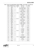
6.6.5. Disabling FS_OUT (Si5366)
The FS_OUT maybe disabled via the DBLFS pin, see Table 29. The additional state (M) provided allows for
FS_OUT to drive a CMOS load while the other clock outputs use a different signal format as specified by the
SFOUT[1:0] pins.
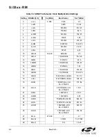
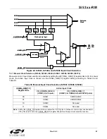
6.7. Output Clock Drivers
The devices include a flexible output driver structure that can drive a variety of loads, including LVPECL, LVDS,
CML, and CMOS formats. The signal format is selected jointly for all outputs using the SFOUT [1:0] pins, which
modify the output common mode and differential signal swing. See Table 4, “DC Characteristics” for output driver
specifications. The SFOUT [1:0] pins are three-level input pins, with the states designated as L (ground), M (V
DD
/
2), and H (V
DD
).
Table 30 shows the signal formats based on the supply voltage and the type of load being driven. For the CMOS
setting (SFOUT = LH), both output pins drive single-ended in-phase signals and should be externally shorted
together to obtain the drive strength specified in Table 4, “DC Characteristics”, see Section
“8.2. Output Clock
Drivers”.
The SFOUT [1:0] pins can also be used to disable the output. Disabling the output puts the CKOUT+ and CKOUT–
pins in a high-impedance state relative to V
DD
(common mode tri-state) while the two outputs remain connected to
each other through a 200
on-chip resistance (differential impedance of 200
). The maximum amount of internal
circuitry is powered down, minimizing power consumption and noise generation. Changing SFOUT without a reset
causes the output to output skew to become random. When SFOUT = LH for CMOS, PLL bypass mode is not
supported.
6.7.1. LVPECL and CMOS TQFP Output Signal Format Restrictions at 3.3 V (Si5365, Si5366)
The LVPECL and CMOS output formats draw more current than either LVDS or CML. However, the allowed output
format pin settings are restricted so that the maximum power dissipation for the TQFP devices is limited when they
are operated at 3.3 V. When SFOUT[1:0] = MH or LH (for either LVPECL or CMOS), either DBL5 must be H or
DBL34 must be high.
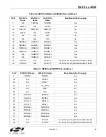
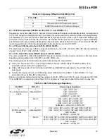
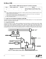
Table 29. FS_OUT Disable Control (DBLFS)
DBLFS
FS_OUT State
H
Tri-State/Powerdown
M
Active/CMOS Format
L
Active/SFOUT[1:0] Format
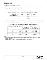
Table 30. Output Signal Format Selection (SFOUT)
SFOUT[1:0]
Signal Format
HL
CML
HM
LVDS
LH
CMOS
LM
Disabled
MH
LVPECL
ML
Low-swing LVDS
All Others
Reserved
Содержание Si5316 Series
Страница 2: ...Si53xx RM 2 Rev 0 52 ...
Страница 109: ...Si53xx RM Rev 0 52 109 8 3 Typical Scope Shots for SFOUT Options Figure 46 sfout_2 CMOS Figure 47 sfout_3 lowSwingLVDS ...
Страница 110: ...Si53xx RM 110 Rev 0 52 Figure 48 sfout_5 LVPECL Figure 49 sfout_6 CML ...
Страница 111: ...Si53xx RM Rev 0 52 111 Figure 50 sfout_7 LVDS ...
Страница 127: ...Si53xx RM Rev 0 52 127 Figure 66 155 52 MHz In 622 08 MHz Out Loop BW 7 Hz Si5324 ...
Страница 128: ...Si53xx RM 128 Rev 0 52 Figure 67 19 44 MHz In 156 25 MHz Out Loop BW 80 Hz ...
Страница 129: ...Si53xx RM Rev 0 52 129 Figure 68 19 44 MHz In 156 25 MHz Out Loop BW 5 Hz Si5324 ...
Страница 130: ...Si53xx RM 130 Rev 0 52 Figure 69 27 MHz In 148 35 MHz Out Light Trace BW 6 Hz Dark Trace BW 110 Hz Si5324 ...
Страница 131: ...Si53xx RM Rev 0 52 131 Figure 70 61 44 MHz In 491 52 MHz Out Loop BW 7 Hz Si5324 ...
Страница 132: ...Si53xx RM 132 Rev 0 52 Figure 71 622 08 MHz In 672 16 MHz Out Loop BW 6 9 kHz ...
Страница 133: ...Si53xx RM Rev 0 52 133 Figure 72 622 08 MHz In 672 16 MHz Out Loop BW 100 Hz ...
Страница 134: ...Si53xx RM 134 Rev 0 52 Figure 73 156 25 MHz In 155 52 MHz Out ...
Страница 139: ...Si53xx RM Rev 0 52 139 Figure 78 86 685 MHz In 173 371 MHz Out ...
Страница 140: ...Si53xx RM 140 Rev 0 52 Figure 79 86 685 MHz In 693 493 MHz Out ...
Страница 142: ...Si53xx RM 142 Rev 0 52 Figure 81 10 MHz In 1 GHz Out ...
Страница 174: ...Si53xx RM 174 Rev 0 52 Figure 99 Si5374 Si5375 DSPLL A ...
Страница 175: ...Si53xx RM Rev 0 52 175 Figure 100 Si5374 Si5375 DSPLL B ...
Страница 176: ...Si53xx RM 176 Rev 0 52 Figure 101 Si5374 Si5375 DSPLL C ...


