


S i 5 3 x x - R M
96
Rev. 0.52
7.11.1.2. Standard LOS (Si5319, Si5324, Si5326, Si5327, Si5368, Si5369, Si5374, Si5375)
To facilitate automatic hitless switching, the LOS trigger time can be significantly reduced by using the default LOS
option (LOSn_EN = 11). The LOS circuitry divides down each input clock to produce a 2 kHz to 2 MHz signal. The
LOS circuitry over samples this divided down input clock using a 40 MHz clock to search for extended periods of
time without input clock transitions. If the LOS monitor detects twice the normal number of samples without a clock
edge, an LOS alarm is declared. The LOSn trigger window is based on the value of the input divider N3. The value
of N3 is reported by DSPLL
sim
.
The range over which LOS is guaranteed to not produce false positive assertions is 100 ppm. For example, if a
device is locked to an input clock on CKIN1, the frequency of CKIN2 should differ by no more than 100 ppm to
avoid false LOS2 assertions.
The frequency range over which FOS monitoring may occur is from 10 to 710 MHz.
7.11.1.3. LOSA (Si5319, Si5324, Si5326, Si5327, Si5368, Si5369, Si5374, Si5375)
A slower response version of LOS called LOSA is available and should be used under certain conditions. Because
LOSA is slower and less sensitive than LOS, its use should be considered for applications with quasi-periodic
clocks (e.g., gapped clocks with one or more consecutive clock edges removed), when switching between input
clocks with a large difference in frequency and any other application where false positive assertions of LOS may
incorrectly cause the Any-Frequency device to be forced into Digital Hold.
For example, one might consider the use of LOSA instead of LOS in Free Run mode applications because the two
clock inputs will not be the same exact frequency. This will avoid false LOS assertions when the XA/XB frequency
differs from the other clock inputs by more than 100 ppm. See Section 7.11.1.3 for more information on LOSA.
7.11.1.4. LOS disabled (Si5319, Si5324, Si5326, Si5327, Si5368, Si5369, Si5374, Si5375)
For situations where no form of LOS is desired, LOS can be disabled by writing 00 to
LOSn_EN
. This mode is
provided to support applications which implement custom LOS algorithms off-chip. If this approach is taken, the
only remaining methods of entering Digital Hold will be FOS or by setting
DHOLD
(register 3, bit 5).
7.11.1.5. Wideband LOS Algorithm (Si5322, Si5365)
Each input clock is divided down to produce a 78 kHz to 1.2 MHz signal before entering the LOS monitoring
circuitry. The same LOS algorithm as described in the above section is then used. FOS is not available in wideband
devices.
7.11.1.6. LOS Alarm Outputs (Si5319, Si5324, Si5325, Si5326, Si5327, Si5367, Si5369, Si5374, Si5375)
When LOS is enabled, an LOS condition on CKIN1 causes
LOS1_INT
to become active. Similarly, when LOS is
enabled, an LOS condition on CKIN2 causes
LOS2_INT
to become active. Once a
LOSn_INT
alarm is asserted on
one of the input clocks, it remains asserted until the input clock is validated over a designated time period. If
another error condition on the same input clock is detected during the validation time then the alarm remains
asserted and the validation time starts over.
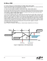
7.11.2. FOS Algorithm (Si5324, Si5325, Si5326, Si5368, Si5369, Si5374)
The frequency offset (FOS) alarms indicate if the input clocks are within a specified frequency range relative to the
frequency of a reference clock. The reference clock can be provided by any of the four input clocks (two for Si5324,
Si5325 or Si5326) or the XA/XB input. The default FOS reference is CKIN2. The frequency monitoring circuitry
compares the frequency of the input clock(s) with the FOS reference clock If the frequency offset of an input clock
exceeds a selected frequency offset threshold, an FOS alarm (
FOS_INT
register bit) is declared for that clock
input. Be aware that large amounts of wander can cause false FOS alarms.
Note:
For the Si5368, If
CK_CONFIG_REG
= 1, only CKIN1 and CKIN2 are monitored; CKIN3 and CKIN4 are used for
FSYNC and are not monitored.
The frequency offset threshold is selectable using the
FOS_THR
[1:0] bits. Settings are available for compatibility
with SONET Minimum Clock (SCMD) or Stratum 3/3E requirements. See Table 8 on page 39. The device supports
FOS hystereses per GR-1244-CORE, making the device less susceptible to FOS alarm chattering. A reference
clock with suitable accuracy and drift specifications to support the intended application should be used. The FOS
reference clock is set via the
FOSREFSEL
[2:0] bits as shown in Table 50. More than one input can be monitored
against the FOS reference, i.e., there can be more than one monitored clock, but only one FOS reference. When
the XA/XB input is used as the FOS reference, there is only one reference frequency band that is allowed: from
37 MHz to 41 MHz.
Содержание Si5316 Series
Страница 2: ...Si53xx RM 2 Rev 0 52 ...
Страница 109: ...Si53xx RM Rev 0 52 109 8 3 Typical Scope Shots for SFOUT Options Figure 46 sfout_2 CMOS Figure 47 sfout_3 lowSwingLVDS ...
Страница 110: ...Si53xx RM 110 Rev 0 52 Figure 48 sfout_5 LVPECL Figure 49 sfout_6 CML ...
Страница 111: ...Si53xx RM Rev 0 52 111 Figure 50 sfout_7 LVDS ...
Страница 127: ...Si53xx RM Rev 0 52 127 Figure 66 155 52 MHz In 622 08 MHz Out Loop BW 7 Hz Si5324 ...
Страница 128: ...Si53xx RM 128 Rev 0 52 Figure 67 19 44 MHz In 156 25 MHz Out Loop BW 80 Hz ...
Страница 129: ...Si53xx RM Rev 0 52 129 Figure 68 19 44 MHz In 156 25 MHz Out Loop BW 5 Hz Si5324 ...
Страница 130: ...Si53xx RM 130 Rev 0 52 Figure 69 27 MHz In 148 35 MHz Out Light Trace BW 6 Hz Dark Trace BW 110 Hz Si5324 ...
Страница 131: ...Si53xx RM Rev 0 52 131 Figure 70 61 44 MHz In 491 52 MHz Out Loop BW 7 Hz Si5324 ...
Страница 132: ...Si53xx RM 132 Rev 0 52 Figure 71 622 08 MHz In 672 16 MHz Out Loop BW 6 9 kHz ...
Страница 133: ...Si53xx RM Rev 0 52 133 Figure 72 622 08 MHz In 672 16 MHz Out Loop BW 100 Hz ...
Страница 134: ...Si53xx RM 134 Rev 0 52 Figure 73 156 25 MHz In 155 52 MHz Out ...
Страница 139: ...Si53xx RM Rev 0 52 139 Figure 78 86 685 MHz In 173 371 MHz Out ...
Страница 140: ...Si53xx RM 140 Rev 0 52 Figure 79 86 685 MHz In 693 493 MHz Out ...
Страница 142: ...Si53xx RM 142 Rev 0 52 Figure 81 10 MHz In 1 GHz Out ...
Страница 174: ...Si53xx RM 174 Rev 0 52 Figure 99 Si5374 Si5375 DSPLL A ...
Страница 175: ...Si53xx RM Rev 0 52 175 Figure 100 Si5374 Si5375 DSPLL B ...
Страница 176: ...Si53xx RM 176 Rev 0 52 Figure 101 Si5374 Si5375 DSPLL C ...


