DX-SX1H
– 52 –
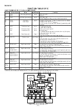
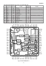
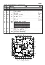
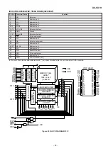
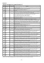
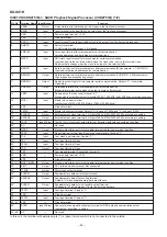
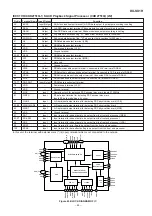
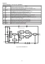
IC602 RH-iX1474GEZZ: SACD Data Processor (IX1474GE) (2/2)
84
DVDD3
—
Digital power supply (3.3V)
For logic cell
85-88
SD3-SD0
Output
MPEG data output
89
SERR
Output
MEPG data reliability flag (Data error = "L")
90
SBGN
Output
MEPG output sector synchronous signal (Sector head = "L")
91
SENB
Output
MEPG data effective flag (Effective = "L")
92
SDCK
Output
MEPG data transfer clock
93
DVSS
—
Digital power supply (0V)
For logic cell
94
SREQ
Input
MEPG data request flag (In case of request = "L")
Level TTL
95
RSTN
Input
Hard reset input (In case of reset = "L")
96
DVDD3
—
Digital power supply (3.3V)
For logic cell
97
STDA
Output
Status data output
98
STCK
Output
Status clock output
99
UPWM
Output
Universal PWM output
100
DVSS
—
Digital power supply (0V)
For logic cell
Pin No.
Terminal
Name
Input/Output
Function
Remarks
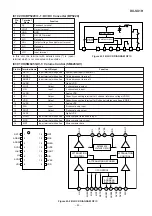
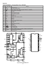
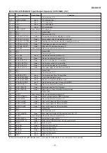
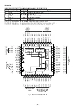
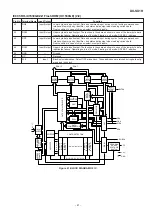
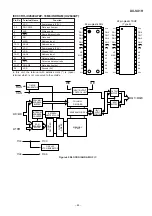
IC603 VHiSC514870SJ: 4Mbit DRAM (SC514870SJ)
Pin No.
Terminal Name
Function
10-13, 16-20, 9
A0-A8, A9R
Address input
8
RAS
Row address strobe
23
CAS
Column address strobe
2-5, 24-27
DQ1-DQ8
Data input/Data output
22
OE
Output enable
7
WE
Write enable
1
VCC
Power supply (5V)
15, 28
VSS
Ground (0V)
6*, 21*
NC
Not used
In this unit, the terminal with asterisk mark (*) is (open)
terminal which is not connected to the outside.
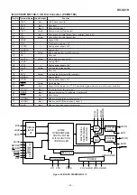
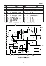
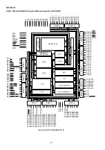
Figure 52 BLOCK DIAGRAM OF IC
Timing
Generator
Timing
Generator
Column
Address
Buffers
Internal
Address
Counter
Row
Address
Buffers
Refresh
Control Clock
Column
Decoders
Sense
Ampliliers
Write
Clock
Generator
I/O
Selector
Output
Buffers
Input
Buffers
Row
De-
coders
Word
Drivers
Memory
Cells
On Chip
Vcc Generator
RAS
CAS
A0 ~ A8
A9R
Vcc
Vcc
Vss
Vss
WE
OE
DO1 ~ DO8
9
9
1
10
9
8
8
8
8
8
8
8

