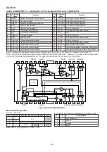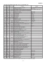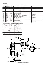
DX-SX1H
– 42 –
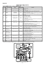
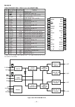
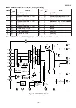
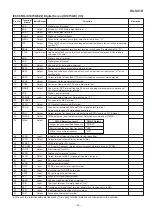
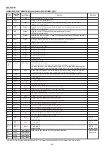
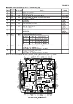
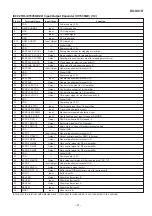
IC201 VHiMN12510F-1: FL Driver (MN12510F)
18
VDD
Power supply terminal
Input
VDD: +5V
±
0.5V
21
VSS
VSS: 0V
16
VPP
FLP driver power supply
Input
VPP: VDD - 35V
Applies voltage to pull-down resistor SEG0-7 and DGT0-7.
19
OSCI
Clock input
Input
Oscillation input terminal
20
OSCO
Clock output
Oscillation output terminal
To OSCI in case of clock input from outside by separately excited
oscillation.
22
NCS
Chip select input
Input
L: Serial input permitted
H: Serial input prohibited
23
SCK
Serial clock input
Input
Clock input for serial transfer
24
SDI
Serial data input
Input
Serial data input:
Command data, address data, indication data, control register
data or port output data is input.
25*
SDO
Serial data output
Output
Serial data output:
Key scan input data or port input data is output.
26*-30*
P30-P34
Key scan input
Input/Output
5 bits.
Can be switched to key scan input, general-purpose input or
general-purpose output by bit unit.
The pull-down resistor is between VSS terminals.
General-purpose output: high current output for driving LED
31-38
SEG0-SEG7
High tension output
Output
8-bit high tension output port. (Segment output)
Output type is Pch open drain, and pull-down resistor is built in
between VPP terminals.
39-42
P10-P13
High tension output
Output
4-bit high tension output port.
SEG8-SEG11
Can be switched to general-purpose output/segment output by bit
unit. Output type is Pch open drain.
43,44,
P20-P23
High tension output
Input/Output
4-bit high tension output port.
1,2
DGT12/SEG15-
Can be switched to general-purpose input/general-purpose output/
DGT15/SEG12
segment output/digit output by bit unit.
Output type is Pch open drain.
High current output for driving LED
3-6
P00-P03
High tension output
Output
4-bit high tension output port.
DGT8-DGT11
Can be switched to general-purpose output/digit output by bit unit.
Output type is Pch open drain.
7-10,
DGT0-DGT7
High tension output
Output
8-bit high tension output port. (Digit output)
12-15
Output type is Pch open drain, and pull-down resistor is built in
between VPP terminals.
11*
NC
—
—
Not used.
Pin No.
Terminal Name
Name
FUNCTION TABLE OF IC
In this unit, the terminal with asterisk mark (*) is (open) terminal which is not connected to the outside.
Input/Output
Function
)
Used to connect ceramic oscillation
terminal.
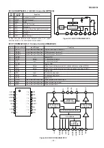
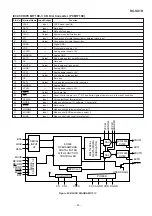
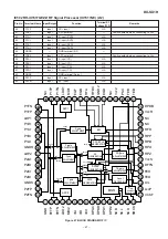
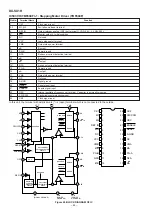
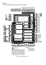
Figure 42 BLOCK DIAGRAM OF IC
S B ( 8 )
L A T C H ( 8 )
LATCH(5)
D G T ( 1 6 )
S E G ( 1 6 )
MPL
MPL
MPL
NCS
SCK
SO1
SO0
VPP
VDD
VSS
OSC1
OSC2
8
8
5
4
4
4
4
4
4
4
4
4
4
K E Y
M A T R I X
F L P
D0
D7D8
D11
S11
S8 S7
S0
P34
P30
DS12
DS15
(P00)
(P03)
(P20)
(P23)
(P13)
(P10)
TIMING
GENERATION
CIRCUIT
INSTRUCTION
DECODER
SHIFT REGISTER
( 8 x 3 2 ) x 2
5 x 1 2

