DX-SX1H
– 54 –
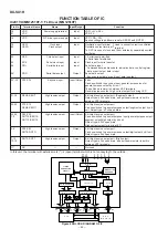
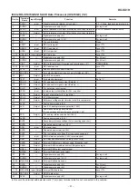
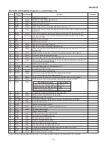
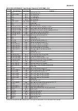
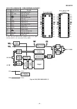
IC606 RH-iX1473GEZZ: Digital Servo (IX1473GE) (2/3)
44
TRO
Output
Tracking equalizer output terminal
45
VREF
—
Analog reference power terminal
46*
RFGC
Output
Outputs 3-pole PWM signal of RF amplitude adjusting signal output terminal.
(PWM carrier = 88.2 kHz)
47
TEBC
Output
Outputs 3-pole PWM signal of tracking balance control signal output terminal.
(PWM carrier = 88.2 kHz)
48
FMO
Output
Outputs 3-pole PWM signal of feed equalizer output terminal.
(PWM carrier = 88.2 kHz)
49*
FVO
Output
Outputs speed error signal or 3-pole PWM signal of feed search EQ output terminal.
(PWM carrier = 88.2 kHz)
50
DMO
Output
To output PWM signals of 3 poles of disc equalizer output terminal.
(PWM carrier = DPS 88.2 kHz, synchronizing with PXO)
51
2VREF
—
Reference power terminal
52
SEL
Output
Laser diode control signal
53
FLGA
Output
FLG-A output terminal
54
FLGB
Output
FLG-B output terminal
55*
FLGC
Output
FLG-C output terminal
56
FLGD
Output
FLG-D output terminal
57
VDD
—
Power terminal
58
VSS
—
Connected to GND.
59-62
IO0-IO3
Input/Output
General-purpose I/O port
(60*)
Can be switched to input/output port possible according to commands.
In case of input port: can read terminal condition (H/L) by read commands possible.
In case of output port: can control terminal condition (H/L/HiZ) by commands possible.
63
/DMOUT
Input
Terminal for setting the mode outputting feed equalizer binary PWM from IO0 and 1
terminals and disc equalizer binary PWM from IO2 and 3 terminals. "L": active.
64
/CKSE
—
X'tal select terminal. In case of 16.9344MHz: "H"; in case of 33.8688 MHz: "L"
65*
/DACT
—
Test terminal
66
TESIN
Input
Test input terminal
67
TESIO1
Input/Output
Test input/output terminal
68
VSS
—
Digital ground terminal
69
PXI
Input
DSP system clock oscillation circuit input terminal
70
PXO
Output
DSP system clock oscillation circuit output terminal
71
VDD
—
D power terminal
72
XVSS
—
Ground terminal for system clock oscillation circuit
73
XI
Input
System clock oscillation circuit input terminal
74*
XO
Output
System clock oscillation circuit output terminal
75
XVDD
—
+ power terminal for system clock oscillation circuit
76
DVDD
—
D/A conversion section power terminal
77*
RO
Output
Channel R data normal rotation output terminal
78
DVSS
—
D/A conversion section analog ground terminal
79
DVR
—
D/A conversion section reference voltage terminal
80*
LO
Output
Channel L data normal rotation output terminal
81
DVDD
—
D/A conversion section power terminal
82
TEST1
Input
Test terminal
Pull-up
Normally open
resistor built in
83
TEST2
Input
Test terminal
Pull-up
Normally open
resistor built in
84
TEST3
Input
Test terminal
Pull-up
Normally open
resistor built in
85
BUS0
Input/Output
Data input/output terminal for microcomputer interface
Schmitt input
86
BUS1
Input/Output
CMOS port
87
BUS2
Input/Output
88
BUS3
Input/Output
Pin No.
Terminal
Name
Input/Output
Function
Remarks
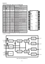
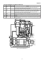
In this unit, the terminal with asterisk mark (*) is (open) terminal which is not connected to the outside.

