60
DV-NC55U/C/M
Name
Type
Description
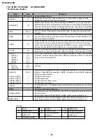
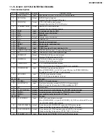
Host interface, CD-DSP interface, sub-code interface (32-pin)
RESET#
ID
Reset input (active Low). When shifting from the assert state to deassert state,
initialization process of this device is started.
Stand-by input (active Low). When asserting with RESET#, all of output pins and
STANDBY#
ID
bidirectional pins enter the float state, and this device is electrically separated from
periphery. All internal operations are stopped and the power consumption is minimized.
In the stand-by mode, the contents of SDRAM and setup parameter are not retained.
IDLE
O(p.u.)
Idle, Init, or Reset state display output (active High). It enters the active state after
resetting.
Data bus width of the host interface is determined. It can be changed during resetting
HWID
ID
only. The host interface of the device is set to 8 bits at the low level (GNDP) and 16
bits at the high level (VDDP).
When the width is 16 bits (HWID is VDDP), byte order of the host interface data bus
HORD
ID
is determined. It can be changed during resetting only. The device is set to input/
output m.s. byte HD at [15:8] at the low level (GNDP), and m.s. byte at [7:0] at the
high level. When HWID is at the GNDP level, it is connected to GNDP.
HTYPE
ID
Protocol of the host bus is determined. It can be changed during resetting only. The
device is set to A type at the low level (GNDP) and B type at the high level (VDDP).
HD[7:0]
I/O
8 I.s. of the host data bus. When HWID input is connected to GNDP, only this signal
(HD[7:4])
(r.t.)
is defined as the host data signal. When HWID is connected to VDDP, it is used as
(HD[3])
(p.u.)
an 8 I.s. line of 16-bit data bus.
(HD[2:1])
(r.t.)
(HD[0])
(p.u.)
HD[11:8]
I/O
When HWID is connected to VDDP, it is used as a data line 11:8 of the 16-bit host
(HD[11])
(p.d.)
data bus.
(HD[10:8])
(r.t.)
When HWID is connected to VDDP, it is used as a data line 15:12 of the 16-bit host
HD[15:12]
I/O(r.t.)
data bus. When HWID is connected to GNDP, it is used as a the CD-DSP serial input
port pin as defined below.
CDCLK (HD[12])
I
CD-DSP bit clock input
CDDAT (HD[13])
I
CD-DSP data input
CDFRM (HD[14)
I
CD-DSP LR clock (frame) input
CDERR (HD[15])
I
CD-DSP data error input
HA[3:0]
I
Host address input. The address signal specifying the physical address in this device
is input.
HCS#
I
Host chip select input. Active Low.
Host protocol A type (HTYPE=GNDP): HR/W#. This input determines the direction of
HWR# (HR/W#)
I
the host access.
Host protocol B type (HTYPE=VDDP): HWR#. Host write input (active Low).
HRD# (HDS)
I
Host protocol A type (HTYPE=GNDP): HDS#. Data strobe input (active Low).
\Host protocol B type (HTYPE=VDDP): HRD#. Host read input (active Low).
Glossary
I
Input
O
Output
I/O
Bidirectional
AI
Analog input
AO
Analog output
AI/O
Analog bidirectional
ID
Input not synchronized
p.u.
Terminal internally
p.d.
Terminal internally
with PCLK
pulled up
pulled down
r.t.
Retained terminal
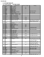
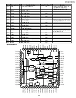
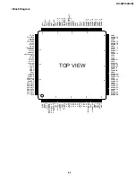
11-6. IC601 IX1720GE
AV DECODER
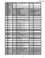
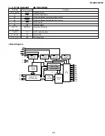
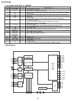
• Terminal description
Содержание DV-NC55C
Страница 75: ...75 DV NC55U C M M E M O ...
Страница 82: ...88 DV NC55U C M A B C D E F G H I J 1 2 3 4 5 6 7 8 9 10 13 3 VTR DISPLAY CIRCUIT SCHEMATIC DIAGRAM ...
Страница 91: ...103 DV NC55U C M 10 11 12 13 14 15 16 17 18 19 A B C D E F G H I J 1 2 3 4 5 6 7 8 9 10 Wiring Side SIDE A ...
Страница 93: ...105 DV NC55U C M 10 11 12 13 14 15 16 17 18 19 A B C D E F G H I J 1 2 3 4 5 6 7 8 9 10 Wiring Side SIDE B ...
Страница 98: ...110 DV NC55U C M A B C D E F G H I J 1 2 3 4 5 6 7 8 9 10 POWER PWB Component Side SIDE A Wiring Side SIDE A ...
Страница 100: ...112 DV NC55U C M A B C D E F G H I J 1 2 3 4 5 6 7 8 9 10 INTERFACE PWB Component Side SIDE A Wiring Side SIDE A ...
Страница 106: ...122 DV NC55U C M A B C D E F G H I J 1 2 3 4 5 6 7 8 9 10 M E M O ...
Страница 127: ...Ref No Part No Description Code Ref No Part No Description Code 143 DV NC55U C M ...

