
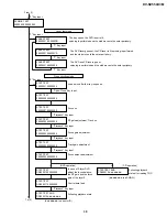
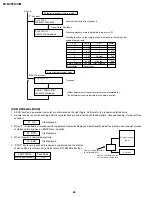

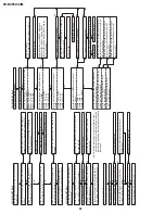
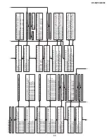


52
DV-NC55U/C/M
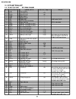
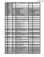
Pin No. Terminal name
I/O
Operation function
Terminal DC Voltage(TYP.)
Remarks
1
GND
–
GND terminal.
–
2
P2TP
I
TE+input (CD)
VrA
3
P2TN
I
TE–input (CD)
VrA
4
LDO2
O
Drive ouput 2
–
5
MDI2
I
Monitor input 2
–
6
VrD
O
Digital VREF
–
Vdd/2 output (1.65V)
7
Vrfil
–
Filter capacity for reference
–
8
Vdd
I
Power terminal
–
3.3V is connected.
9
DPAC
–
DPD AC combination capacity 1
–
10
DPBD
–
DPD AC combination capacity 2
–
11
DPD1
–
DPD integral capacity 1
–
12
DPD2
–
DPD integral capacity 2
–
13
SCB
I
Control line (Bit clock)
2.2[V]
14
SCL
I
Control line (Latch signal)
2.2[V]
15
SCD
I
Control line (Sirial Data)
2.2[V]
16
VRCK
I
Reference clock input
2.3[V]
When frequency is increased, the
filters excepting the servo LPF are
shifted to high frequency side.
17
VCKF
–
Capacity for VRCK time constant
–
adjustment
18
VccP
–
Power terminal
–
19
LVL
O
Servo addition output
VrD/2
20
TEO
O
TE output
VrD
21
FEO
O
FE output
VrD
22
DFTN
I
DPD difect
–
Low DPD output: Mute
23
VccS
–
Power terminal (servo)
–
24
NC
–
–
–
Used in the open state.
25
RPZ
O
RF ripple output 2
VrD
26
RPO
O
RF ripple output 1
VrD/2
27
RPB
–
RF ripple bottom
–
28
RPP
–
RF ripple peak
–
29
RFOn
O
Equivalent RF output
1.65[V]
DC voltage varies by RFS.
(Differential output)
30
RFOp
O
Equivalent RF output
1.65[V]
DC voltage varies by RFS.
(Differential output)
31
VccR
–
Power terminal (RF)
–
32
RFS
I
RF slice level adjustment
–
33
TEB
I
TE balance
VrD
When TEB is raised, the gain on the
TP side and the delay amount on the
A+C side are increased.
Adjusting range: GND - Vdd
34
FEB
I
FE balance
VrD
When FEB is raised, the gain on the
A+C (FP) side is increased.
Adjusting range: GND - Vdd
35
DPDB
I
Pit depth adjustment
VrD
When DPDB is raised, the delay
amount on the A•B side is increased.
Adjusting range: GND - Vdd
36
Vcc2
–
Power terminal
–
37
NC
–
–
–
Used in the open state.
38
NC
–
–
–
Used in the open state.
39
GND2
–
GND terminal.
–
40
TCC1
I
Time constant adjustment
–
41
RFDC
–
DC feedback capacity
–
42
VrA
O
Analog VREF
2.1[V]
43
EQB
I
Boost adjustment
VrD
When EQB is raised, the boost increases.
Adjusting range: GND - Vdd
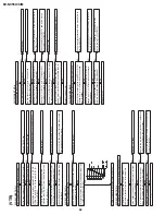
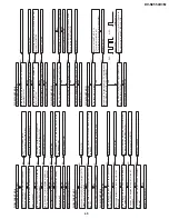
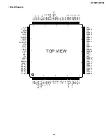
11. IC FUNCTION LIST
11-1. IC301 TA1323F
RF PROCESSOR
Содержание DV-NC55C
Страница 75: ...75 DV NC55U C M M E M O ...
Страница 82: ...88 DV NC55U C M A B C D E F G H I J 1 2 3 4 5 6 7 8 9 10 13 3 VTR DISPLAY CIRCUIT SCHEMATIC DIAGRAM ...
Страница 91: ...103 DV NC55U C M 10 11 12 13 14 15 16 17 18 19 A B C D E F G H I J 1 2 3 4 5 6 7 8 9 10 Wiring Side SIDE A ...
Страница 93: ...105 DV NC55U C M 10 11 12 13 14 15 16 17 18 19 A B C D E F G H I J 1 2 3 4 5 6 7 8 9 10 Wiring Side SIDE B ...
Страница 98: ...110 DV NC55U C M A B C D E F G H I J 1 2 3 4 5 6 7 8 9 10 POWER PWB Component Side SIDE A Wiring Side SIDE A ...
Страница 100: ...112 DV NC55U C M A B C D E F G H I J 1 2 3 4 5 6 7 8 9 10 INTERFACE PWB Component Side SIDE A Wiring Side SIDE A ...
Страница 106: ...122 DV NC55U C M A B C D E F G H I J 1 2 3 4 5 6 7 8 9 10 M E M O ...
Страница 127: ...Ref No Part No Description Code Ref No Part No Description Code 143 DV NC55U C M ...


