69
4. TROUBLESHOOTING
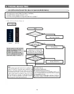
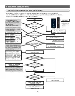
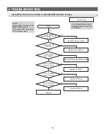
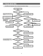
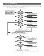
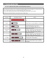
4-2-15) Troubleshooting based on LED Blinking Frequency
When the Failure Condition occurs, the Compressor will immediately stop if the Compressor is running and there will
be a 5 minute standby. During the 5 minute standby, RPM signals will be ignored.
That is, even though the Inverter PCB receives the RPM signals, the Compressor does not work.
It blinks every second and there is 2 second off at the end of each cycle.
Description
LED Blinking Frequency
Remark
Normal Operation
N/A
Failure
Check if there is any short between Comp terminals.
IPM Fault
Check IPM Voltage [lower than 13.5V].
Check any short between IPM Pins [#1~33].
Location Detect
Failure
Check Comp and Cycle.
Check the continuity of the following resistances for
Short/Open (R505, R506, R507, R508, R509, R510,
R511, R512, R513) Check Comp. Connector.
Motor Restriction
Check Comp and Cycle.
Check the continuity of the following resistances for
Short/Open (R505, R506, R507, R508, R509, R510,
R511, R512, R513) Check Comp and Cycle.
Low Voltage
When the Input Voltage is under AC110V Check the
continuity of R517 for Short/Open
Over Voltage
When the Input Voltage is higher than AC300V,
check the continuity of R514, R515 and R516 for
Short/Open
Содержание RL60GG Series
Страница 12: ...12 2 PRODUCT SPECIFICATIONS 592 1201 7 595 500 584 675 712 2010 2 4 Dimensions mm RL60 RL58 RL56 2010 1920 1850...
Страница 75: ...75 5 PCB DIAGRAM 5 3 Connector Layout and Description Main Board 5 3 1 Q G J OPTION...
Страница 76: ...76 5 PCB DIAGRAM 5 3 2 R P Z H Option...
Страница 77: ...77 5 PCB DIAGRAM 5 3 3 L Option...
Страница 78: ...78 5 PCB DIAGRAM 5 3 4 W E Option...
Страница 80: ...80 5 PCB DIAGRAM IPM DIODE VOLTAGE 5 5 IPM Diode Voltage...
Страница 81: ...81 6 WIRING DIAGRAM 6 1 Q G J OPTION...
Страница 82: ...82 6 WIRING DIAGRAM 6 2 R P Z H Option...
Страница 83: ...83 6 WIRING DIAGRAM 6 3 L Option...
Страница 84: ...84 6 WIRING DIAGRAM 6 4 W E Option...
Страница 85: ...85 6 WIRING DIAGRAM 6 5 S Option...
Страница 86: ...86 7 CIRCUIT DIAGRAM 7 1 Schematic Diagram PBA Main 7 1 1 Q G J OPTION...
Страница 87: ...87 7 CIRCUIT DIAGRAM 7 1 2 R P Z H L Option...
Страница 88: ...88 7 CIRCUIT DIAGRAM 7 1 3 W E S Option...
Страница 89: ...89 7 CIRCUIT DIAGRAM 7 2 Schematic Diagram PBA Inverter...
Страница 90: ...90 7 CIRCUIT DIAGRAM 7 3 Block Diagram PBA Main...
Страница 91: ...91 7 CIRCUIT DIAGRAM 7 4 Block Diagram PBA Inverter G H L P R Z Option...
Страница 92: ...92 7 CIRCUIT DIAGRAM 7 5 Block Diagram PBA Inverter Q J Option...
Страница 93: ...93 8 REFERENCE INFORMATION 9 2 Nomenclatrue...

