65
4. TROUBLESHOOTING
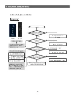
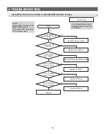
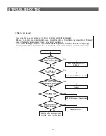
The connector at the
Freezer upper hinge cover
is inserted properly.
MAIN PCB Connector
(CN52, CN51) is
inserted properly
There are no buttons
being pressed
continuously.
DOOR PANEL PCB
Connector is inserted
properly
The trouble continues
with PCB being
removed
It lights up when
PANEL-PCB is being
replaced
When PANEL-PCB is
being replaced, it
works normal.
Start
Re-insert Connector,
Correct the defective contact
Re-insert MAIN PCB Connector
Re-assemble PCB ASS'Y, Correct
any restrictions on the buttons
Re-insert Connector,
Correct the defective contact
Re-assemble PCB ASS'Y, Correct
any restrictions on the buttons
Defective PANEL PCB
Defective PANEL PCB
No
No
Being Pressed
When PANEL KEY is
not selected
No
When being separated, it works
Yes
Yes
Yes
Yes
Yes
Yes
Yes
No
No
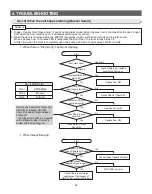
Refer to Circuit Diagram
attached in this manual and
check the circuit diagram
attached on the back of the
unit.
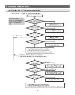
①
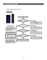
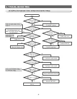
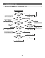
When PANEL PCB does not light up or partially does
②
When Panel PCB buttons are not working
※
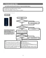
When the trouble is being remained after the above,
①
Check Fridge Door Wiring - Short or Open Wire
②
Check CABI Upper Wiring - Short or Open Wire
③
Check Short/Open at MAIN PCB Panel Lamp Circuit
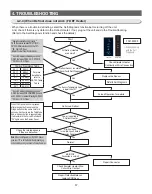
①
Check Fridge Door Wire - Short or Open Wire
②
Check CABI Upper Wiring - Short or Open Wire
③
Check Short/Open at MAIN PCB Panel Communication/Power-Supply Circuit
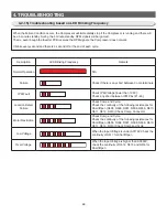
4-2-11) When PANEL PCB operates abnormally
Содержание RL60GG Series
Страница 12: ...12 2 PRODUCT SPECIFICATIONS 592 1201 7 595 500 584 675 712 2010 2 4 Dimensions mm RL60 RL58 RL56 2010 1920 1850...
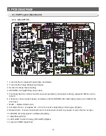
Страница 75: ...75 5 PCB DIAGRAM 5 3 Connector Layout and Description Main Board 5 3 1 Q G J OPTION...
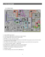
Страница 76: ...76 5 PCB DIAGRAM 5 3 2 R P Z H Option...
Страница 77: ...77 5 PCB DIAGRAM 5 3 3 L Option...
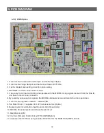
Страница 78: ...78 5 PCB DIAGRAM 5 3 4 W E Option...
Страница 80: ...80 5 PCB DIAGRAM IPM DIODE VOLTAGE 5 5 IPM Diode Voltage...
Страница 81: ...81 6 WIRING DIAGRAM 6 1 Q G J OPTION...
Страница 82: ...82 6 WIRING DIAGRAM 6 2 R P Z H Option...
Страница 83: ...83 6 WIRING DIAGRAM 6 3 L Option...
Страница 84: ...84 6 WIRING DIAGRAM 6 4 W E Option...
Страница 85: ...85 6 WIRING DIAGRAM 6 5 S Option...
Страница 86: ...86 7 CIRCUIT DIAGRAM 7 1 Schematic Diagram PBA Main 7 1 1 Q G J OPTION...
Страница 87: ...87 7 CIRCUIT DIAGRAM 7 1 2 R P Z H L Option...
Страница 88: ...88 7 CIRCUIT DIAGRAM 7 1 3 W E S Option...
Страница 89: ...89 7 CIRCUIT DIAGRAM 7 2 Schematic Diagram PBA Inverter...
Страница 90: ...90 7 CIRCUIT DIAGRAM 7 3 Block Diagram PBA Main...
Страница 91: ...91 7 CIRCUIT DIAGRAM 7 4 Block Diagram PBA Inverter G H L P R Z Option...
Страница 92: ...92 7 CIRCUIT DIAGRAM 7 5 Block Diagram PBA Inverter Q J Option...
Страница 93: ...93 8 REFERENCE INFORMATION 9 2 Nomenclatrue...


