40
4. TROUBLESHOOTING
4-1-3) Load Status Display Function
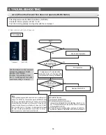
1) At the normal operation, press the F Fridge buttons for 6 seconds.
Then, the Freezer and Freezer Temperature Display will blink in an interval of 0.5 second for 4 seconds.
2) At this time, release the F Fridge buttons and press the Alarm button (it sends out "Ding Dong"
sound.) Then, it shifts to the Load Display mode.
3) The Load Display function shows what MICOM signals come out from MAIN PCB.
But, it just indicates that there are MICOM signals coming out.
It does not necessarily mean that the related parts (Loads) are operating.
In other word, even though it shows a certain load working, the related part may not operate due to such
as a defective PCB relay or the defective part itself (it needs a confirmation).
4) The Load Display function lasts for 30 seconds and then it goes back to the normal operation.
5) The following image shows load locations with the 7-segment LEDs.
②
①
Press the F Fridge
buttons for 6 seconds at the
same time, and while the Display
LEDs are blinking for 4 seconds,
release the buttons and
②
Press the Alarm button once.
BAR-TYPE
7-Segment
①
Содержание RL60GG Series
Страница 12: ...12 2 PRODUCT SPECIFICATIONS 592 1201 7 595 500 584 675 712 2010 2 4 Dimensions mm RL60 RL58 RL56 2010 1920 1850...
Страница 75: ...75 5 PCB DIAGRAM 5 3 Connector Layout and Description Main Board 5 3 1 Q G J OPTION...
Страница 76: ...76 5 PCB DIAGRAM 5 3 2 R P Z H Option...
Страница 77: ...77 5 PCB DIAGRAM 5 3 3 L Option...
Страница 78: ...78 5 PCB DIAGRAM 5 3 4 W E Option...
Страница 80: ...80 5 PCB DIAGRAM IPM DIODE VOLTAGE 5 5 IPM Diode Voltage...
Страница 81: ...81 6 WIRING DIAGRAM 6 1 Q G J OPTION...
Страница 82: ...82 6 WIRING DIAGRAM 6 2 R P Z H Option...
Страница 83: ...83 6 WIRING DIAGRAM 6 3 L Option...
Страница 84: ...84 6 WIRING DIAGRAM 6 4 W E Option...
Страница 85: ...85 6 WIRING DIAGRAM 6 5 S Option...
Страница 86: ...86 7 CIRCUIT DIAGRAM 7 1 Schematic Diagram PBA Main 7 1 1 Q G J OPTION...
Страница 87: ...87 7 CIRCUIT DIAGRAM 7 1 2 R P Z H L Option...
Страница 88: ...88 7 CIRCUIT DIAGRAM 7 1 3 W E S Option...
Страница 89: ...89 7 CIRCUIT DIAGRAM 7 2 Schematic Diagram PBA Inverter...
Страница 90: ...90 7 CIRCUIT DIAGRAM 7 3 Block Diagram PBA Main...
Страница 91: ...91 7 CIRCUIT DIAGRAM 7 4 Block Diagram PBA Inverter G H L P R Z Option...
Страница 92: ...92 7 CIRCUIT DIAGRAM 7 5 Block Diagram PBA Inverter Q J Option...
Страница 93: ...93 8 REFERENCE INFORMATION 9 2 Nomenclatrue...


