56
4. TROUBLESHOOTING
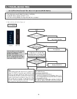
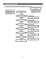
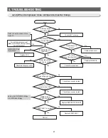
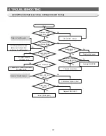
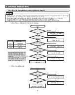
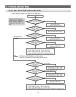
4-2-3) When the C-Fan does not operate (BLDC Motor)
- This refrigerator uses the BLDC Fan Motor. (OPTION)
The BLDC Motor operates with DC 7~12V.
- The F-Fan motor generally runs together with the compressor.
The Compressor is Off.
It reads DC7~12
between MAIN PCB
GND and CN72 #8
It repeats DC7~12V,
and DC 2V or lower between MAIN PCB GND
and CN72 PIN #8
Start
Run Forced Operation
FAN operates.
Replace MAIN PCB
No
Yes
No
Yes
Yes
Yes
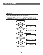
Note
Pulse signals being generated when the motor is rotating are
to be input to CN72 #8 (C). These will be input to MICOM and
when there are no input signals with the motor rotating, the fan
will be turned off and then be turned on in 10 seconds. If there
are still no input signals, it keeps trying the above 4 times. And,
if it still fails, it runs the motor in 10 minutes. It is implemented to
prevent the motor from being overloaded due to restrictions by
foreign substances such as ice built up around the motor.
Upon the initial power on, the compressor
and the C-Fan operate.
But, when there is an instance power
failure, it operates with the operation of
the compressor.
Apply power in 7 minutes after
turning the motor off. (To prevent the
compressor from being overloaded)
◆
Possible Causes
①
Defective FAN-MOTOR
②
Contact problem at the terminal
(MAIN PCB CONNECTOR-TERMINAL (CN72.
⑦
,
⑧
,
⑩
), Contact problem at Freezer Fan Motor Connector,
Defective Motor Wire)
③
Check the motor rotating pulse input upon Fan Motor
operation. (Refer to Fan-Motor Circuit in this manual)
No
☞
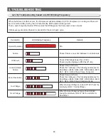
When checking with the Self Diagnosis
C FAN ERROR
No
BAR-TYPE
7-Segment
Содержание RL60GG Series
Страница 12: ...12 2 PRODUCT SPECIFICATIONS 592 1201 7 595 500 584 675 712 2010 2 4 Dimensions mm RL60 RL58 RL56 2010 1920 1850...
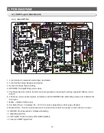
Страница 75: ...75 5 PCB DIAGRAM 5 3 Connector Layout and Description Main Board 5 3 1 Q G J OPTION...
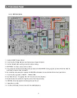
Страница 76: ...76 5 PCB DIAGRAM 5 3 2 R P Z H Option...
Страница 77: ...77 5 PCB DIAGRAM 5 3 3 L Option...
Страница 78: ...78 5 PCB DIAGRAM 5 3 4 W E Option...
Страница 80: ...80 5 PCB DIAGRAM IPM DIODE VOLTAGE 5 5 IPM Diode Voltage...
Страница 81: ...81 6 WIRING DIAGRAM 6 1 Q G J OPTION...
Страница 82: ...82 6 WIRING DIAGRAM 6 2 R P Z H Option...
Страница 83: ...83 6 WIRING DIAGRAM 6 3 L Option...
Страница 84: ...84 6 WIRING DIAGRAM 6 4 W E Option...
Страница 85: ...85 6 WIRING DIAGRAM 6 5 S Option...
Страница 86: ...86 7 CIRCUIT DIAGRAM 7 1 Schematic Diagram PBA Main 7 1 1 Q G J OPTION...
Страница 87: ...87 7 CIRCUIT DIAGRAM 7 1 2 R P Z H L Option...
Страница 88: ...88 7 CIRCUIT DIAGRAM 7 1 3 W E S Option...
Страница 89: ...89 7 CIRCUIT DIAGRAM 7 2 Schematic Diagram PBA Inverter...
Страница 90: ...90 7 CIRCUIT DIAGRAM 7 3 Block Diagram PBA Main...
Страница 91: ...91 7 CIRCUIT DIAGRAM 7 4 Block Diagram PBA Inverter G H L P R Z Option...
Страница 92: ...92 7 CIRCUIT DIAGRAM 7 5 Block Diagram PBA Inverter Q J Option...
Страница 93: ...93 8 REFERENCE INFORMATION 9 2 Nomenclatrue...


