R01UH0823EJ0100 Rev.1.00
Page 124 of 1823
Jul 31, 2019
RX23W Group
5. I/O Registers
000A 007Ch
USB0
PIPE7 Control Register
PIPE7CTR
16
16
9 PCLKB
or more
Frequency
with 1 + 9 ×
(frequency
ratio of ICLK/
PCLKB)*
000A 007Eh
USB0
PIPE8 Control Register
PIPE8CTR
16
16
9 PCLKB
or more
Frequency
with 1 + 9 ×
(frequency
ratio of ICLK/
PCLKB)*
000A 0080h
USB0
PIPE9 Control Register
PIPE9CTR
16
16
9 PCLKB
or more
Frequency
with 1 + 9 ×
(frequency
ratio of ICLK/
PCLKB)*
000A 0090h
USB0
PIPE1 Transaction Counter Enable Register
PIPE1TRE
16
16
9 PCLKB
or more
Frequency
with 1 + 9 ×
(frequency
ratio of ICLK/
PCLKB)*
000A 0092h
USB0
PIPE1 Transaction Counter Register
PIPE1TRN
16
16
9 PCLKB
or more
Frequency
with 1 + 9 ×
(frequency
ratio of ICLK/
PCLKB)*
000A 0094h
USB0
PIPE2 Transaction Counter Enable Register
PIPE2TRE
16
16
9 PCLKB
or more
Frequency
with 1 + 9 ×
(frequency
ratio of ICLK/
PCLKB)*
000A 0096h
USB0
PIPE2 Transaction Counter Register
PIPE2TRN
16
16
9 PCLKB
or more
Frequency
with 1 + 9 ×
(frequency
ratio of ICLK/
PCLKB)*
000A 0098h
USB0
PIPE3 Transaction Counter Enable Register
PIPE3TRE
16
16
9 PCLKB
or more
Frequency
with 1 + 9 ×
(frequency
ratio of ICLK/
PCLKB)*
000A 009Ah
USB0
PIPE3 Transaction Counter Register
PIPE3TRN
16
16
9 PCLKB
or more
Frequency
with 1 + 9 ×
(frequency
ratio of ICLK/
PCLKB)*
000A 009Ch
USB0
PIPE4 Transaction Counter Enable Register
PIPE4TRE
16
16
9 PCLKB
or more
Frequency
with 1 + 9 ×
(frequency
ratio of ICLK/
PCLKB)*
000A 009Eh
USB0
PIPE4 Transaction Counter Register
PIPE4TRN
16
16
9 PCLKB
or more
Frequency
with 1 + 9 ×
(frequency
ratio of ICLK/
PCLKB)*
000A 00A0h
USB0
PIPE5 Transaction Counter Enable Register
PIPE5TRE
16
16
9 PCLKB
or more
Frequency
with 1 + 9 ×
(frequency
ratio of ICLK/
PCLKB)*
000A 00A2h
USB0
PIPE5 Transaction Counter Register
PIPE5TRN
16
16
9 PCLKB
or more
Frequency
with 1 + 9 ×
(frequency
ratio of ICLK/
PCLKB)*
000A 00B0h
USB0
BC Control Register 0
USBBCCTRL0
16
16
9 PCLKB
or more
Frequency
with 1 + 9 ×
(frequency
ratio of ICLK/
PCLKB)*
000A 00CCh
USB0
USB Module Control Register
USBMC
16
16
9 PCLKB
or more
Frequency
with 1 + 9 ×
(frequency
ratio of ICLK/
PCLKB)*
000A 00D0h
USB0
Device Address 0 Configuration Register
DEVADD0
16
16
9 PCLKB
or more
Frequency
with 1 + 9 ×
(frequency
ratio of ICLK/
PCLKB)*
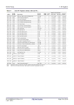
Table 5.1
List of I/O Registers (Address Order) (20/31)
Address
Module
Symbol
Register Name
Register
Symbol
Number
of Bits
Access
Size
Number of Access Cycles
Reference
Section
ICLK
PCLK
ICLK <PCLK


