R01UH0092EJ0110 Rev.1.10
Page 426 of 807
Jul 31, 2012
M16C/64C Group
22. Remote Control Signal Receiver
22.3.1.2
PMCi Input
The options below can be selected in PMCi input (see Figure 22.2 “Remote Control Signal Receiver
Block Diagram (2/3) (PMCi Input)”).
•
Input pin
•
Input polarity
•
Digital filter
A pin to which the PMCi signal is input is selected by setting bits PSEL1 to PSEL0 in the PMCiCON2
register.
To process the signal input to the PMC0 pin in the PMC1 circuit, or to process the signal input to the
PMC1 pin in the PMC0 circuit, use the same count source in PMC0 and PMC1.
(refer to 22.3.1.1 “Count Source”).
Input polarity of the PMCi pin can be inverted. Whether to invert or not can be selected by setting the
SINV bit in the PMCiCON0 register.
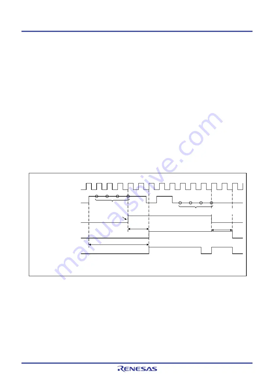
If the signal input to the PMCi pin holds the same level for four sequential cycles when the FIL bit in
the PMCiCON0 register is 1 (digital filter enabled), that level is transferred to the internal circuit. The
sampling clock of the digital filter is the count source.
Select bits CSRC1 to CSRC0 (count source) in the PMC0CON3 register and bits CDIV1 to CDIV0
(count source divisor) before selecting bits PSEL1 to PSEL0 (input pin), the FIL bit (digital filter), and
the SINV bit (input signal polarity invert). Input to the PMCi pin is transferred to the internal circuit in
synchronization with the count source. Internal processing causes a delay. Figure 22.5 shows PMCi
Input Delay.
Figure 22.5
PMCi Input Delay
Sampling clock
(count source)
Internal processing (5 to 6 cycles)
Internal
processing
Internal
processing
(2 cycles)
PMCi pin input
Digital filter output
(internal signal)
FIL = 1 (digital filter enabled)
PMCi internal input signal
FIL = 0 (digital filter disabled)
i = 0, 1
FIL: Bit in the PMCiCON0 register
Holds the same
level for four
sequential cycles
Holds the same level for four sequential cycles
Содержание M16C Series
Страница 846: ...M16C 64C Group R01UH0092EJ0110...


