PDP-5010FD
58
1
2
3
4
1
2
3
4
C
D
F
A
B
E
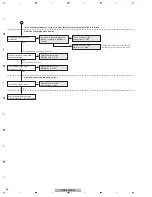
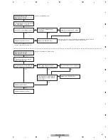
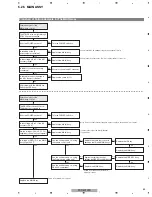
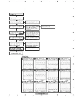
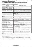
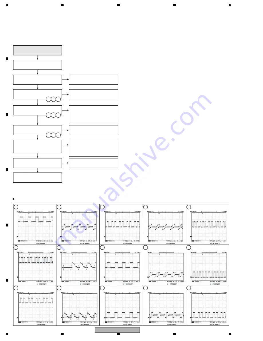
Is the function corresponding to
selected signal input selected?
Select the corresponding signal
with the input selector.
No
Check the communication between
the CN4701 and around IC4901.
No
Check the circuit between IC4701 and
IC5001 and replace broken parts.
No
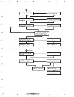
The panel is defective.
No
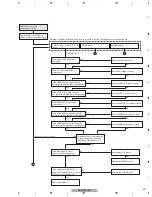
Check around IC4701 and check the
communications between IC4701
and the microcomputer. If there was
no ploblem replace IC4701.
No
Check around the IC that is found to
have a failure in communication and
the microcomputer. If there was no
ploblem replace MAIN Assy.
No
Replace the MAIN Assy.
Yes
Yes
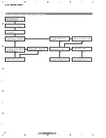
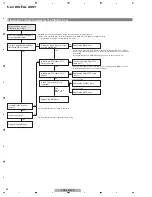
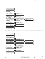
Image for the PC signal is not
displayed.
=> PC
Has the signal arrived at IC4701?
(pins 30, 32, 34)
Yes
Is a signal output from IC4701?
(pin 41, 43, 45)
Has the signal arrived at IC5001?
(pin 43, 48, 54)
Yes
Has the symptom been settled
when the MAIN Assy is replaced?
Yes
Yes
Is the communication between
each IC on the MAIN Assy and
the microcomputer nomal?
Yes
15
18
14
13
12
11
10
17
16
13
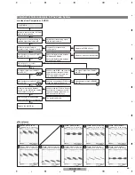
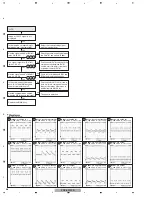
IC4701 - pin 30 (component_PR)
V: 500 mV/div H: 10
μ
sec/div
13
IC4701 - pin 30 (PC_R)
V: 500 mV/div H: 10
μ
sec/div
15
IC4701 - pin 34 (component_Y)
V: 500 mV/div H: 10
μ
sec/div
15
IC4701 - pin 34 (PC_G)
V: 500 mV/div H: 10
μ
sec/div
17
IC5001 - pin 48 (component)
V: 500 mV/div H: 10
μ
sec/div
17
IC5001 - pin 48 (PC)
V: 500 mV/div H: 20
μ
sec/div
14
IC4701 - pin 32 (component_Pb)
V: 500 mV/div H: 10
μ
sec/div
14
IC4701 - pin 32 (PC_B)
V: 500 mV/div H: 10
μ
sec/div
16
IC5001 - pin 43 (component)
V: 500 mV/div H: 10
μ
sec/div
16
IC5001 - pin 43 (PC)
V: 500 mV/div H: 10
μ
sec/div
18
IC5001 - pin 54 (component)
V: 500 mV/div H: 20
μ
sec/div
18
IC5001 - pin 54 (PC)
V: 500 mV/div H: 20
μ
sec/div
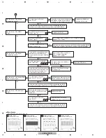
11
IC4701 - pin 66 (PC_B)
V: 500 mV/div H: 20
μ
sec/div
12
IC4701 - pin 68 (PC_R)
V: 500 mV/div H: 20
μ
sec/div
Waveforms
Input signal: Color-bar
10
IC4701 - pin 64 (PC_G)
V: 500 mV/div H: 20
μ
sec/div
Содержание PDP-5010FD
Страница 19: ...PDP 5010FD 19 5 6 7 8 5 6 7 8 C D F A B E ...
Страница 20: ...PDP 5010FD 20 1 2 3 4 1 2 3 4 C D F A B E 4 BLOCK DIAGRAM 4 1 OVERALL WIRING DIAGRAM 1 2 ...
Страница 22: ...PDP 5010FD 22 1 2 3 4 1 2 3 4 C D F A B E 4 2 OVERALL WIRING DIAGRAM 2 2 V 8V_AU V 3_3V_A V 3_3V_AU_D ...
Страница 23: ...PDP 5010FD 23 5 6 7 8 5 6 7 8 C D F A B E ...
Страница 35: ...PDP 5010FD 35 5 6 7 8 5 6 7 8 C D F A B E ...
Страница 167: ...PDP 5010FD 167 5 6 7 8 5 6 7 8 C D F A B E ...
Страница 178: ...PDP 5010FD 178 1 2 3 4 1 2 3 4 C D F A B E 10 6 PANEL CHASSIS SECTION ...
Страница 182: ...PDP 5010FD 182 1 2 3 4 1 2 3 4 C D F A B E 10 8 PDP SERVICE ASSY 508F AWU1272 Exterior Section ...


