Appendix D: Breadboarding Rules
· Page 313
P15
P14
P13
P12
P11
P10
P9
P8
P7
P6
P5
P4
P3
P2
P1
P0
X2
X3
Vdd
Vss
Vin
Vdd
Vss
LED
470
Ω
+
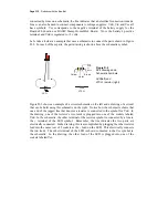
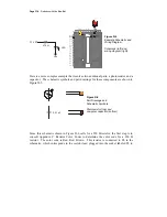
Figure D-3
Example Schematic and
Wiring Diagram
Schematic (left) and wiring
diagram (right)
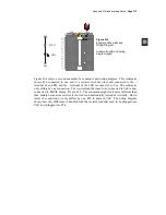
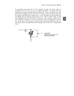
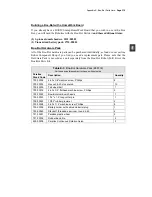
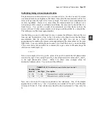
Figure D-4 shows a second example of a schematic and wiring diagram. This schematic
shows P14 connected to one end of a resistor, with the other end connected to the +
terminal of an LED, and the – terminal of the LED is connected to Vss. The schematic
only differs by one connection. The resistor lead that used to be connected to Vdd is now
connected to BASIC Stamp I/O pin P14. The schematic might look more different than
that, mainly because the resistor is shown drawn horizontally instead of vertically. But in
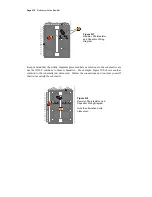
terms of connections, it only differs by one, P14 in place of Vdd. The wiring diagram
shows how this difference is handled with the resistor lead that used to be plugged into
Vdd, now plugged into P14.


