


NXP Semiconductors
UM11729
FRDMGD3162HBIEVM half-bridge evaluation board
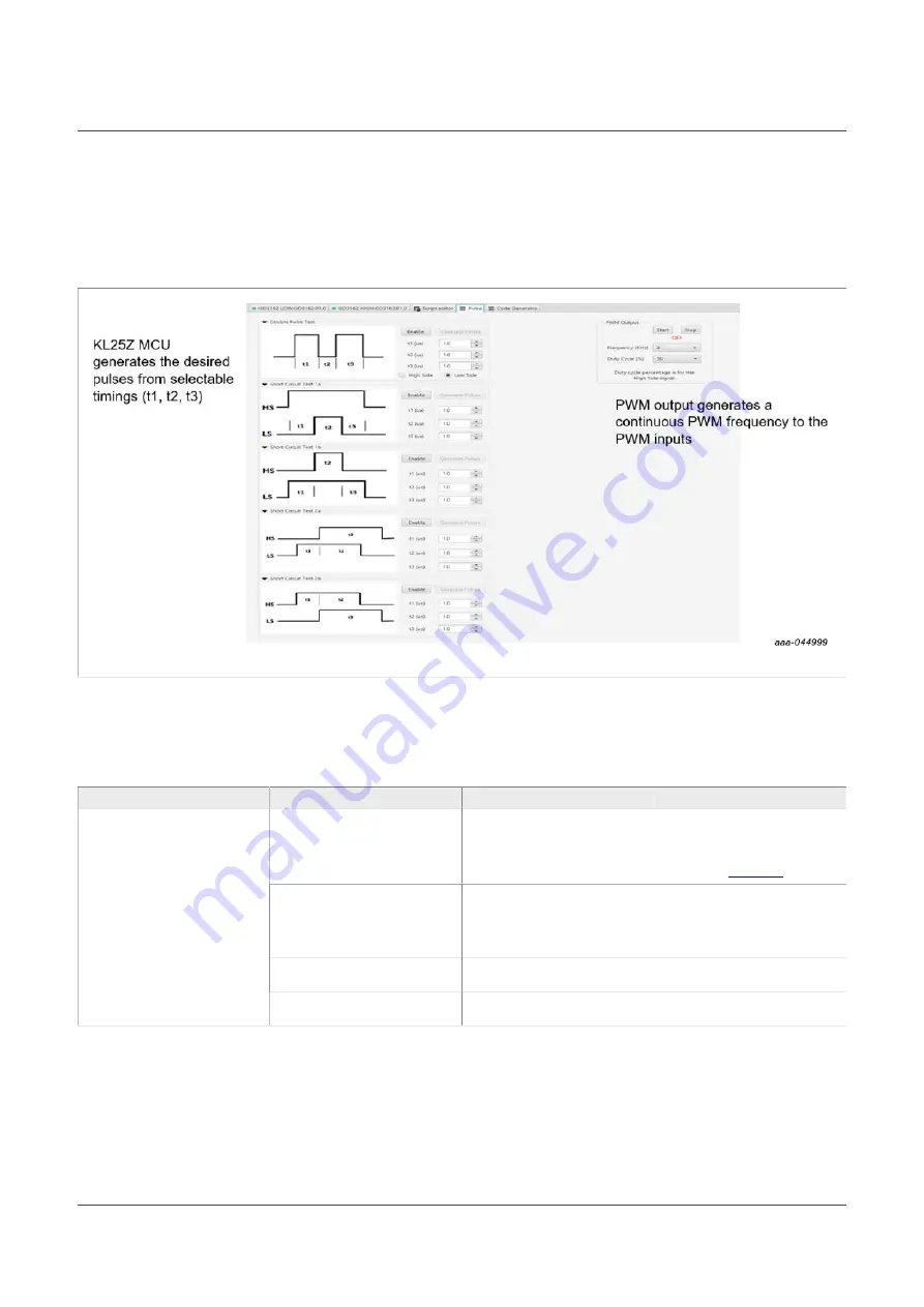
Pulse tab
•
Used for double pulse, short circuit, and PWM testing
•
Select desired T1, T2, and T3 timings for each test type; select enable then generate
pulses
Figure 34. Pulse tab
6.4 Troubleshooting
Some common issues and troubleshooting procedures are detailed below. This is not an
exhaustive list by any means, and additional debug may be needed:
Problem
Evaluation
Explanation
Corrective action(s)
Check PWM jumper position on
translator board
Incorrect PWM jumpers obstruct
signal path but not report fault
Set PWMH_SEL (J4) and
PWML_SEL (J5) jumpers properly, for
desired control method:
•
3.3 V to 5.0 V translator board
Check PWM control signal
Ensure that proper PWM signal is
reaching GD3162
Monitor PWML (TP11) and PWMH
(TP10) on translator board for
commanded PWM state. Check
position of jumpers J4 and J5 on
translator board.
Check FSENB status (see GD3162
pin 15, STATUS3)
PWM is disabled when
FSENB = LOW
Set pin FSENB = HIGH (pin 15) to
continue
No PWM output (no fault reported)
Check CONFIG_EN bit (MODE2)
PWM is disabled when
CONFIG_EN is logic 1
Write CONFIG_EN = logic 0 to
continue
UM11729
All information provided in this document is subject to legal disclaimers.
© NXP B.V. 2022. All rights reserved.
User manual
Rev. 1 — 21 February 2022
37 / 43