


Appendix A
Specifications
A-2
ni.com
NI PXI-4220 Accuracy Information
Maximum Working Voltage
( common-mode) .......................Either the S
X
+ (pin 1) or
S
X
– (pin 6) input should remain
within ±10 V of ground. Both
inputs should remain within
±10 V of each other. Maximum
working voltage refers to the
signal voltage plus the common
mode voltage.
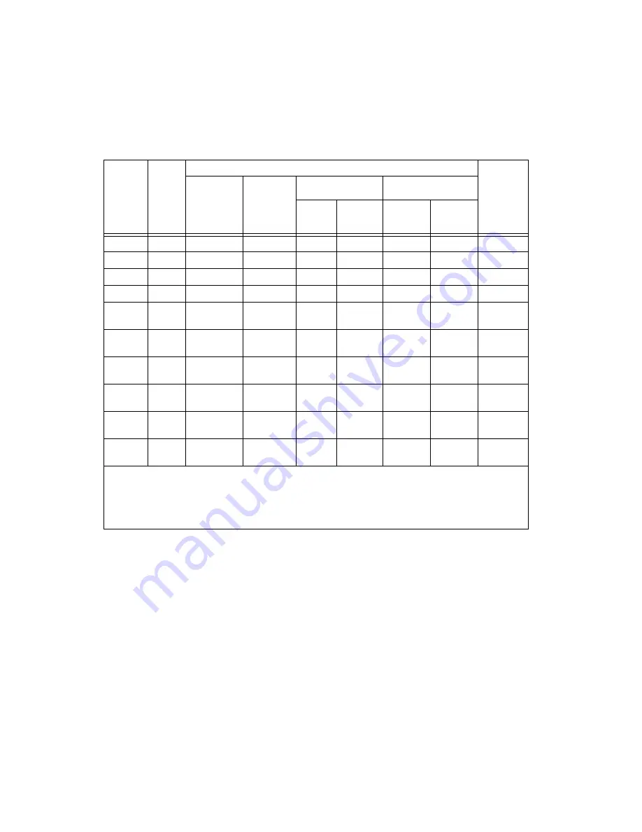
Nominal
Range
Gain
Absolute Accuracy
Absolute
Accuracy at
Full Scale
% of Reading
1 Year
Maximum
Offset (
µ
V)
Noise + Quantization
(
µ
V)
Temperature Drift
Single
Pt.
Averaged
Gain Drift
(%/
°
C)
Offset
Drift
(
µ
/
°
C)
±10.0 V
1
0.1
3000
5000
500
0.0300
25.00
±13.5 mV
±5.0 V
2
0.1
1500
2500
250
0.0300
25.00
±6.8 mV
±1.8 V
4.2
0.1
500
1000
100
0.0300
25.00
±2.4 mV
±1.0 V
10
0.1
300
500
50
0.0300
25.00
±1.4 mV
±500.0
mV
20
0.1
150
250
25
0.0300
5.00
±675
µ
V
±180.0
mV
42
0.1
75
100
10
0.0300
5.00
±265
µ
V
±100.0
mV
100
0.1
50
50
5.0
0.0300
5.00
±155
µ
V
±50.0
mV
200
0.1
50
25
2.5
0.0300
5.00
±103
µ
V
±18.0
mV
420
0.1
50
10
1.0
0.0300
5.00
±69
µ
V
±10.0
mV
1000
0.1
50
10
1.0
0.0300
5.00
±61
µ
V
Accuracies are valid for measurements following an internal self-calibration and using the 10 Hz filter setting. Averaged numbers assume an
average of 100 single-channel readings.
Measurement accuracies are listed for operational temperatures within ±1 °C of internal calibration temperature and ±10 °C of external or
factory calibration temperature.
The absolute accuracy at full scale calculations use the maximum range input voltage (for example 10 V on the ±10 V range) at one year
accuracy, assuming averaged data.


