©
National Instruments Corporation
3-1
3
Hardware Overview
This chapter presents an overview of the hardware functions on your 1408
device and explains the operation of each functional unit making up the
1408 device.
Functional Overview
The 1408 device features an 8-bit flash ADC that converts video signals
to digital formats, four video signal multiplexers, and programmable gain
and offset. It also uses a PCI interface for high-speed data transfer,
scatter-gather DMA controllers that control the transfer of data between the
first-in, first-out (FIFO) memory buffers and the PCI bus, nonvolatile and
static RAM for configuring registers on power-up and programming the
DMA controllers, and acquisition and region-of-interest control circuitry
that monitors video signals. The board also includes powerful trigger
circuitry including four external triggers and RTSI bus triggers. Other
features include internally generated or externally input CSYNC, HSYNC,
VSYNC, and PCLK synchronization and clock signals.
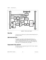
The block diagram in Figure 3-1 illustrates the key functional components
of the 1408 device.


