


–
R
= rank(s)
–
xff
= Device organization (data bit width) of SDRAMs used on this assembly
• x4 = x4 organization (4 DQ lines per SDRAM)
• x8 = x8 organization
• x16 = x16 organization
–
wwwww
is the DIMM bandwidth, in MBps: 2133, 2400, 2666, 2933, 3200
–
aa
is the SDRAM speed grade
–
m
is the DIMM type
– E = Unbuffered DIMM (UDIMM), x64 p 8 bit ECC module data bus
– L = Load Reduced DIMM (LRDIMM), x64 p 8 bit ECC module data bus
– R = Registered DIMM (RDIMM), x64 p 8 bit ECC module data bus
– U = Unbuffered DIMM (UDIMM) with no ECC (x64-bit primary data bus)
–
cc
is the reference design file used for this design
–
d
is the revision number of the reference design used
–
bb
is the JEDEC SPD Revision Encoding and Additions level used on this DIMM
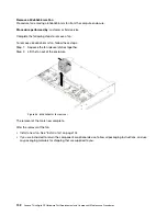
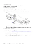
The following illustration shows the location of the DIMM connectors on the system board.
Figure 54. Location of the DIMM connectors on the system board
.
Part replacement and maintenance procedures
113
Содержание ThinkAgile CP
Страница 4: ...ii Lenovo ThinkAgile CP Hardware Part Replacement and Component Maintenance Procedures ...
Страница 6: ...iv Lenovo ThinkAgile CP Hardware Part Replacement and Component Maintenance Procedures ...
Страница 8: ...vi Lenovo ThinkAgile CP Hardware Part Replacement and Component Maintenance Procedures ...
Страница 30: ...22 Lenovo ThinkAgile CP Hardware Part Replacement and Component Maintenance Procedures ...
Страница 33: ...Chapter 4 Managing Support Mode 25 ...
Страница 80: ...72 Lenovo ThinkAgile CP Hardware Part Replacement and Component Maintenance Procedures ...
Страница 158: ...150 Lenovo ThinkAgile CP Hardware Part Replacement and Component Maintenance Procedures ...
Страница 160: ...152 Lenovo ThinkAgile CP Hardware Part Replacement and Component Maintenance Procedures ...
Страница 161: ......
Страница 162: ......