5 Configuration Mode Introduction
5.9 I2C Mode
UG290-2.3E
69(87)
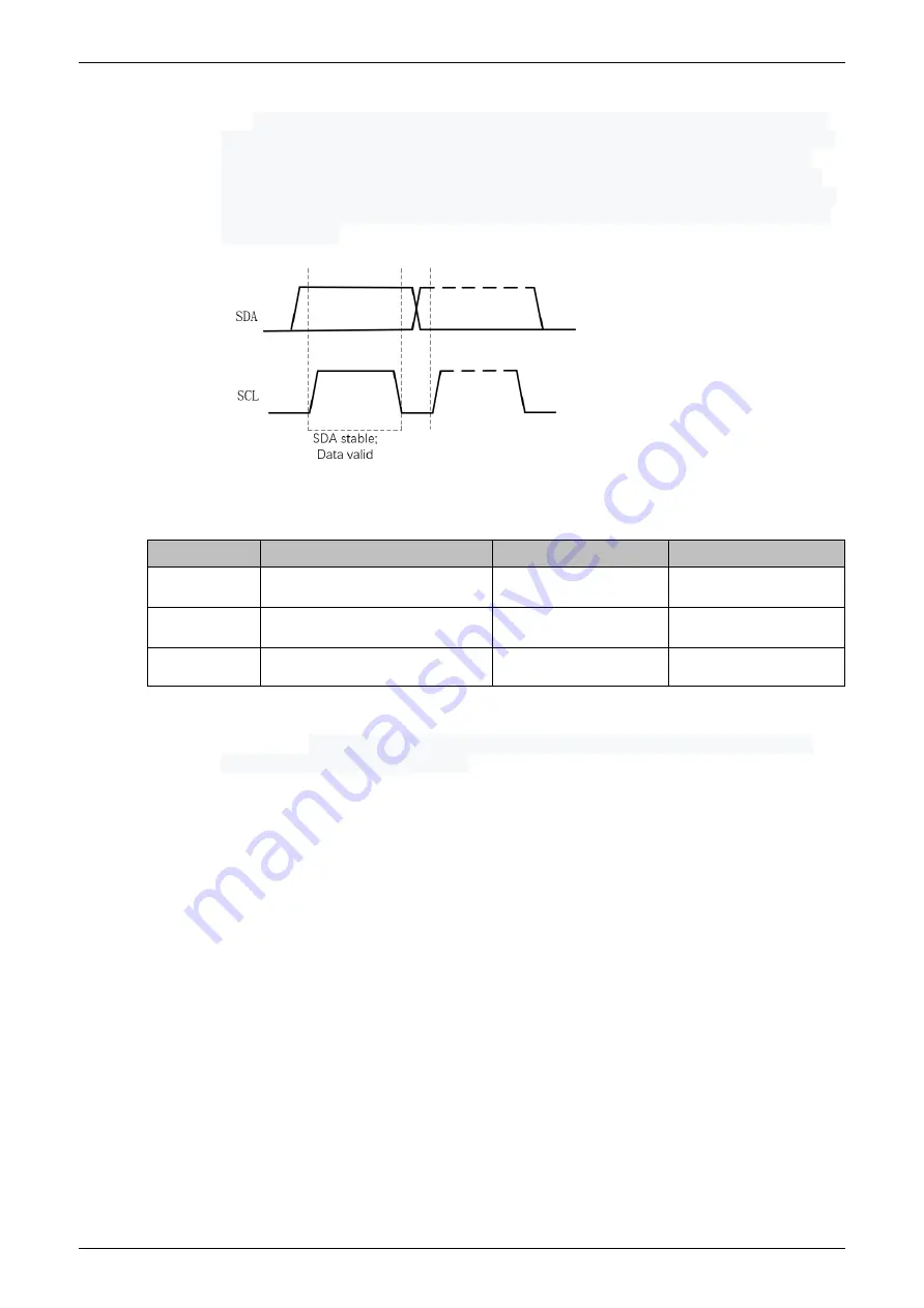
Each bit of data transmitted on the I2C bus has a corresponding clock pulse (or
synchronous control), that is, each bit of data is transmitted serially on the SDA bit by
bit based on the SCL serial clock. During data transfer, the level on the SDA must
remain stable, with the low level being data 0 and the high level being data 1, while
the SCL is high.The level on the SDA is allowed to change state only while the SCL is
low.Logic 0 has a low voltage level and Logic 1 has a high voltage level.As shown in
the figure below.
The list of I
2
C mode supported by Gowin FPGA devices is as shown in
the table below.
Mode
Device
Frequency
Address
SRAM
GW1N-2
(
IDCode:0x0120681B
)
100Khz~1.33Mhz
7'b1010_000
Embedded
Flash
GW1N-2
(
IDCode:0x0120681B
)
1.33Mhz
±
1%
7'b1011_000
External
Flash
Note!
If you use I
2
C to write Flash, the bitstream file needs to be conveted into specific bitstream
file first. The
conversion tool is included in Gowin Programmer, and the name after
conversion is suffixed with ". I2C ".
Other than the power requirements, the following conditions need to
be met to use the I
2
C configuration mode:
I
2
C port enable
RECONFIG_N is not set as a GPIO during the first configuration after
power up or the previous programming.
Initiate new configuration
Power-on again or trigger RECONFIG_N at one low pulse.


