


90
90
90
90
Appendix
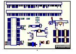
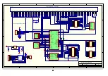
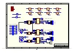
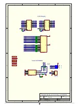
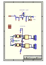
Here you will find schematics of the CPU board for
MB90F543, the Main board schematics, Interface bus and
Device Bus description
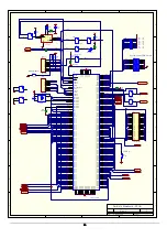
Device Bus (K2) and Interface Bus (K1 ) connectors pins:
DIN Conn.
PIN
Device Bus
Interface Bus
PIN NO.
CPU Pin Nr.
Function
CPU PIN Nr.
SIGNAL
2nd Function
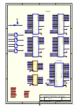
A1
18
SOT0
85
AD00
P00
B1
19
SCK0
86
AD01
P01
C1
20
SIN0
87
AD02
P02
A2
24
SOT1
88
AD03
P03
B2
22
SCK1
89
AD04
P04
C2
21
SIN1
90
AD05
P05
A3
91
AD06
P06
B3
92
AD07
P07
C3
93
AD08
P10
A4
69
INT0
94
AD09
P11
B4
70
INT1
95
AD10
P12
C4
71
INT2
96
AD11
P13
A5
72
INT3
97
AD12
P14
B5
29
INT4
98
AD13
P15
C5
30
INT5
99
AD14
P16
A6
31
INT6
100
AD15
P17
B6
32
INT7
1
A16
P20
C6
25
SOT2
2
A17
P21
A7
26
SCK2
3
A18
P22
B7
28
SIN2
4
A19
P23
C7
5
A20
P24
A8
6
A21
P25
B8
7
A22
P26
C8
8
A23
P27
A9
9
ALE
P30
B9
10
\RD
P31
C9
12
\WRL
P32
A10
13
\WRH
P33
Chapter
15


