F800 CIRCUIT DESCRIPTION
12 (25)
Uppgjord (även faktaansvarig om annan) -
Prepared (also subject responsible if other)
Nr
-
No.
KL/ECS/S/LT Magnus Lindahl
ECS/S/LT-96:5044
Dokansv/Godk -
Doc respons/Approved
Kontr
-
Checked
Datum
-
Date
Rev
File
KI/ECS/S/LTC
1996-06-06
A
965044.DOC
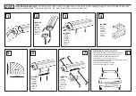
Even in the F800 transmitter a SWR 2:1 is acceptable before the RF power control
loop starts to decrease the output power. The method used in F800 is a combination
of a true SWR measurement and a maximal allowed reversed power. The same signal
as used in the RF power monitor is also connected to a comparator in the RF power
control loop. The signal from the directional coupler that represents the RF output
power is also connected to the same input on the comparator in the RF power control
loop. The two signals are added to each other and the result is a DC value that
represents the RF output power plus the reversed RF power. This complex signal is
then compared with a set value that represents the desired output power level. The
signal that represents the desired output power is decreased when the reversed
power is too high and thus the output power is also reduced. The output from the
comparator in the power control loop is connected to a buffer stage. The buffer stage
acts as a variable resistor and changes the DC supply voltage to the transistor in the
RF driver.
The desired RF output is set in two levels, low = 2 W and high = 20 W. With a logical
control signal, power red, the CPU board can select either high or low output power.
As soon as the transmitter is switched on and the frequency generator is locked, the
power control loop is active. With the logical signal, one of two DC values is connected
to a buffer stage. From the output of the buffer stage the signal is connected to the
SWR comparator as a reference value. In the "desired output power" voltage chain
there is also a temperature depending resistor implemented. The output power is
reduced when the temperature is higher then approximately 60° centigrade. At 90° the
output is reduced by 10 dB to approximately 2 Watts.
The transmitter is supplied with DC as soon as the radio unit is switched on. The transmitter is set in transmission
mode by the TX ON signal from the CPU board. The TX ON signal activates the RF power control
loop.
-
+
+
Power
control
-
+
V
Ref
RF Out
Power
Indication
Temp sense
Power adjust
FIG G: Power control and SWR circuits, principal diagram