


S1F71200 Series
S1F70000 Series
EPSON
4–47
Technical Manual
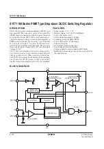
S1F71200
Series
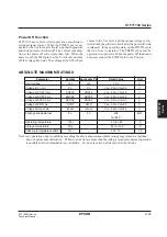
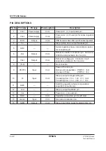
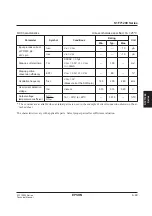
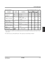
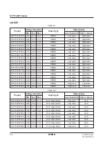
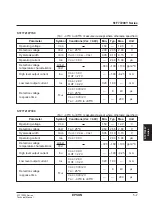
ABSOLUTE MAXIMUM RATINGS
Symbol
V
DD
EXO
V
O
SRC
I
REF
V
REF
POFFX
V
C
SWC
V
SW
SSC
I
SENSE
SWO
P
D
T
opr
T
stg
T
sol
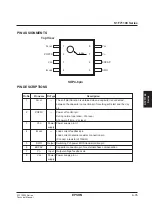
Applicable Pin
V
DD1
V
DD2
EXO
V
O
SRC
I
REF
V
REF
POFFX
V
C
SWC
V
SW
SSC
I
SENSE
SWO
P
D
—
—
—
Rating
15.0
V
SS
– 0.3 to V
DD2
+ 0.3
V
SS
– 0.3 to 15
V
SS
– 0.3 to 15
V
SS
– 0.3 to V
DD1
+ 0.3
V
SS
– 0.3 to V
DD1
+ 0.3
V
SS
– 0.3 to V
DD1
+ 0.3
V
SS
– 0.3 to V
DD1
+ 0.3
V
SS
– 0.3 to 15
V
SS
– 0.3 to 15
V
SS
– 0.3 to V
DD1
+ 0.3
V
SS
– 0.3 to V
DD1
+ 0.3
V
SS
– 0.3 to V
DD1
+ 0.3
210
Ta
≤
25
°
C
–30 to +85
–55 to +150
260 · 10
Unit
V
V
V
V
V
V
V
V
V
V
V
V
V
MW
°
C
°
C
°
C · s
Note
Any operation under conditions exceeding the above absolute maximum ratings may result in a malfunction or a
permanent destruction. When even an item is more than the rating, a temporary normal operation is possible but
with remarkably low reliability. So, be sure to keep all items below the ratings.
Parameter
Input voltage
Voltage at EXO pin
Voltage at V
O
pin
Voltage at SRC pin
Voltage at I
REF
pin
Voltage at V
REF
pin
Voltage at POFFX pin
Voltage at V
C
pin
Voltage at SWC pin
Voltage at V
SW
pin
Voltage at SSC pin
I
SENSE
SWO
Package allowable loss
Operating temperature
Storage temperature
Soldering temperature and time
Содержание S1F76610C0B0
Страница 4: ...S1F70000 Series Technical Manual ...
Страница 17: ...1 DC DC Converter ...
Страница 43: ...2 DC DC Converter Voltage Regulator ...
Страница 107: ...3 Voltage Regulator ...
Страница 145: ...4 DC DC Switching Regulators ...
Страница 200: ...5 Voltage Detector ...
Страница 223: ...6 Appendix ...


