


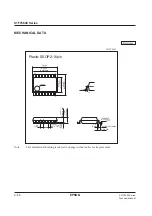
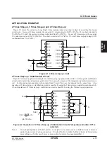

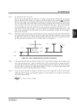
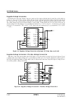


S1F76640 Series
2–46
EPSON
S1F70000 Series
Technical Manual
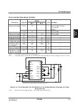
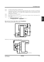
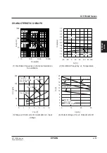
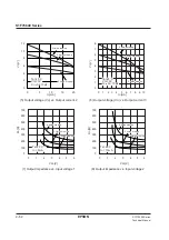
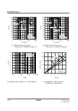
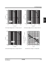
ELECTRICAL CHARACTERISTICS
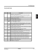
Absolute Maximum Ratings
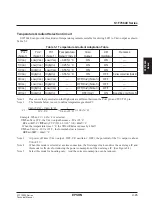
Parameter
Symbol
Rating
Unit
Remarks
Min.
Max.
Input supply voltage
V
DD
GND-0.3
24/N
V
V
DD
N = 2 : 2 times step-up
N = 3 : 3 times step-up
N = 4 : 4 times step-up
Input pin voltage
V
I
GND–0.3
V
DD
-0.3
V
OSC1,P
OFF
GND–0.3
V
O
-0.3
V
TC1,TC2, RV
Output voltage
V
O
GND–0.3
22
V
V
O
Note 3
GND–0.3
V
O
V
V
REG
Note 3
Output pin voltage 1
VOC1
GND–0.3
V
DD
–0.3
V
CAP1+,CAP2+ OSC2
Output pin voltage 2
VOC2
GND–0.3
2
×
V
DD
–0.3
V
CAP1–
Output pin voltage 3
VOC3
GND–0.3
3
×
V
DD
–0.3
V
CAP2–
Output pin voltage 4
VOC4
GND–0.3
4
×
V
DD
–0.3
V
CAP3–
Allowable loss
P
D
—
210
mW
SSOP-16PIN
Operating temperature
Topr
–40
85
˚C
—
Storage temperature
Tstg
–55
150
˚C
—
Soldering
Tsol
—
260
⋅
10
˚C
⋅
s
At leads
temperature and time
Note 1 :
Under the conditions exceeding the above absolute maximum ratings, the IC may result in a permanent
destruction. An operation for a long period under the conditions of the above absolute maximum ratings
may deteriorate the reliability remarkably.
Note 2 :
All voltage values are based on GND.
Note 3 :
The output pins (V
O
and V
REG
) are for stabilizing and outputting boosted voltages. So, they are not
used to apply voltage from outside. When voltage is applied from outside for unavoidable reasons, limit
the voltage to the rated voltage mentioned above or less.
Содержание S1F76610C0B0
Страница 4: ...S1F70000 Series Technical Manual ...
Страница 17: ...1 DC DC Converter ...
Страница 43: ...2 DC DC Converter Voltage Regulator ...
Страница 107: ...3 Voltage Regulator ...
Страница 145: ...4 DC DC Switching Regulators ...
Страница 200: ...5 Voltage Detector ...
Страница 223: ...6 Appendix ...


