


S1F77200Y Series
5–4
EPSON
S1F70000 Series
Technical Manual
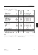
PIN DESCRIPTIONS
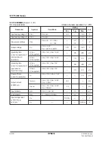
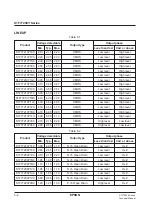
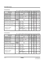
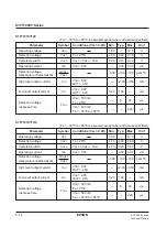
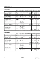
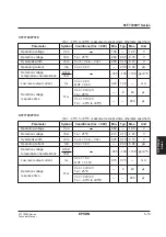
Pin No. Pin name
Description
1
OUT
Voltage detection output pin
2
V
DD
Input voltage pin (positive side)
3
V
SS
Input voltage pin (negative side)
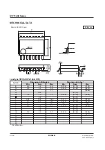
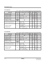
PIN ASSIGNMENTS
SOT89-3pin
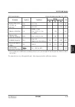
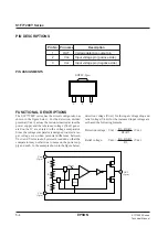
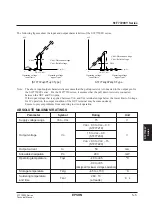
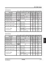
FUNCTIONAL DESCRIPTIONS
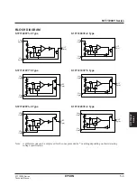
The S1F77200Y series has the circuit configuration as
shown in the figure below. For the detection, divided
potential (V
REG
) across the resistors inserted across the
power supply and the reference voltage (V
REF
) gener-
ated on the IC are entered to the voltage comparator.
Since the voltage comparator is designed to detect a tar-
get voltage even when potential difference between
V
REG
and Vref minute, hysteresis is added so that the
comparator may not fail due to noise on the power sup-
ply and such. In the example shown in the figure below,
detection voltage (V
DET
) for the input voltage drop and
relief voltage (V
REL
) for the increased input voltage are
set based the following formula.
Detection voltage: V
DET
=
R1+R2+R3
• V
REF
R2+R3
Relief voltage:
V
REL
=
R1+R2+R3
• V
REF
R3
1
3
2
V
DD
(2pin)
V
SS
(3pin)
OUT
(1pin)
T
R1
R3
R2
+
—
T
(V
REG
)
V
REF
Содержание S1F76610C0B0
Страница 4: ...S1F70000 Series Technical Manual ...
Страница 17: ...1 DC DC Converter ...
Страница 43: ...2 DC DC Converter Voltage Regulator ...
Страница 107: ...3 Voltage Regulator ...
Страница 145: ...4 DC DC Switching Regulators ...
Страница 200: ...5 Voltage Detector ...
Страница 223: ...6 Appendix ...


