


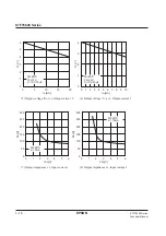
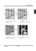
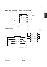

S1F76620 Series
1–12
EPSON
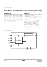
S1F70000 Series
Technical Manual
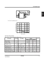
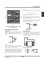
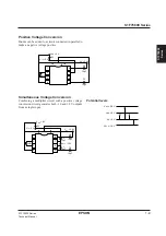
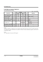
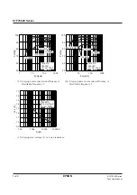
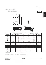
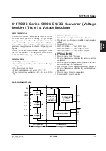
Pad Center Coordinates (S1F76620D0A0)
Chip External Shape
Y
X
+
(0,0)
2.60mm
2.30mm
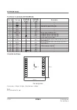
Pad Assignment
Pad aperture : 100
µ
m
×
100
µ
m Chip thickness : 400
µ
m
Note
Do not bond the NC pad.
Pad No.
1
2
3
4
5
6
7
8
9
10
11
12
13
14
15
16
17
Pad name
(NC)
(NC)
P
OFF
(NC)
(NC)
(NC)
GND (V
SS
)
OSC1
OSC2
V
DD
CAP1–
CAP1+
(NC)
V
O
(NC)
(NC)
(NC)
Pad center
coordinates
X (
µ
m)
–984
984
Pad center
coordinates
Y (
µ
m)
1096
788
580
390
96
–218
–510
–802
–1094
–1134
–892
–514
182
372
750
942
1134
Description
—
—
Input pin for power off control
—
—
—
Power input pin (Minus side)
Oscillation resistor connection pin
Oscillation resistor connection pin
Power input pin (Plus side)
Pump up capacitor minus side connection pin for 2
times step-up
Pump up capacitor plus side connection pin for 2
times step-up
—
2 times step-up output pin
—
—
—
Содержание S1F76610C0B0
Страница 4: ...S1F70000 Series Technical Manual ...
Страница 17: ...1 DC DC Converter ...
Страница 43: ...2 DC DC Converter Voltage Regulator ...
Страница 107: ...3 Voltage Regulator ...
Страница 145: ...4 DC DC Switching Regulators ...
Страница 200: ...5 Voltage Detector ...
Страница 223: ...6 Appendix ...


