


MFC-8440/8840D/8840DN, DCP-8040/8045D/8045DN
SERVICE MANUAL
A-47
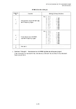
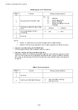
WSW45 (Speeding up scanning-2)
Selector
No.
Function
Setting and Specifications
1
|
3
Delay time from when documents
are set until the ADF starts drawing
them in
No. 1 2 3
0 0 0 : No automatic drawing-in
0
0
1
: 1
sec.
0
1
0
: 2
sec.
0
1
1
: 3
sec.
1
0
0
: 4
sec.
1
0
1
: 5
sec.
1
1
0
: 6
sec.
1
1
1
: 7
sec.
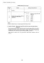
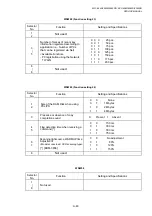
4
|
6
Periodical correction intervals of the
reference voltage to be applied to
white level compensation for
document scanning, during standby
No. 4 5 6
0 0 0 : No correction of reference
voltage
during
standby
0
0
1
:
10
sec.
0
1
0
:
30
sec.
0
1
1
: 1
min.
1
0
0
: 3
min.
1
0
1
: 5
min.
1
1
0
:
10
min.
1
1
1
:
30
min.
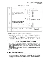
7
Standby position of the CCD unit
0: CCD lock position
1: Location of
(Home position)
the white-level
reference
film
8
Not used.
NOTE:
WSW45 is applicable only to models equipped with a flat-bed scanner.
l
Selectors 1 through 3: Delay time from when documents are set until the ADF starts drawing
them in
These selectors determine how long the ADF will delay automatic drawing-in of documents
(to the scanning standby position) after you set them in the ADF, as well as determining
whether or not the ADF automatically draws in documents.
l
Selectors 4 through 6: Periodical correction intervals of the reference voltage applied to white
level compensation for document scanning, during standby
These selectors set the correction intervals (in seconds) of the reference voltage to be
applied to white level compensation for document scanning during standby, as well as
determining whether or not the controller makes the reference voltage correction during
standby. (Conventionally, the correction has been made immediately before the start of
actual scanning)
This function takes effect in copying. Making the correction during standby may shorten the
preparation time for copying.
NOTE:
Do not access these selectors.
l
Selector 7: Standby position of the CCD unit
This selector determines whether the standby position of the CCD unit should be the CCD
lock position (home position) or the location of the white-level reference film (attached to the
inside of the scanner top cover). If the location of the reference film is selected, the CCD unit
will not return to the lock position so as to shorten the travel time, decreasing the preparation
time for copying.
Содержание DCP-8040
Страница 146: ...CHAPTER 4 DISASSEMBLY AND RE ASSEMBLY 4 64 5 Remove the shutter arm C Fig 4 115 Shutter arm C Frame L ...
Страница 276: ...CHAPTER 7 MAINTENANCE MODE 7 6 Fig 7 3 l m a b c d e f g h i j k ...
Страница 347: ...APPENDIX 4 CIRCUIT DIAGRAMS A 50 Appendix 4 1 Main PCB Circuit Diagram 1 7 ...
Страница 348: ...MFC 8440 8840D 8840DN DCP 8040 8045D 8045DN SERVICE MANUAL A 51 Appendix 4 2 Main PCB Circuit Diagram 2 7 ...
Страница 349: ...APPENDIX 4 CIRCUIT DIAGRAMS A 52 Appendix 4 3 Main PCB Circuit Diagram 3 7 ...
Страница 350: ...MFC 8440 8840D 8840DN DCP 8040 8045D 8045DN SERVICE MANUAL A 53 Appendix 4 4 Main PCB Circuit Diagram 4 7 ...
Страница 351: ...APPENDIX 4 CIRCUIT DIAGRAMS A 54 Appendix 4 5 Main PCB Circuit Diagram 5 7 ...
Страница 352: ...MFC 8440 8840D 8840DN DCP 8040 8045D 8045DN SERVICE MANUAL A 55 Appendix 4 6 Main PCB Circuit Diagram 6 7 ...
Страница 353: ...APPENDIX 4 CIRCUIT DIAGRAMS A 56 Appendix 4 7 Main PCB Circuit Diagram 7 7 ...
Страница 354: ...MFC 8440 8840D 8840DN DCP 8040 8045D 8045DN SERVICE MANUAL A 57 Appendix 4 8 Driver PCB Circuit Diagram ...
Страница 355: ...APPENDIX 4 CIRCUIT DIAGRAMS A 58 Appendix 4 9 Engine PCB Circuit Diagram 1 2 ...
Страница 356: ...MFC 8440 8840D 8840DN DCP 8040 8045D 8045DN SERVICE MANUAL A 59 Appendix 4 10 Engine PCB Circuit Diagram 2 2 ...
Страница 357: ...APPENDIX 4 CIRCUIT DIAGRAMS A 60 Appendix 4 11 NCU PCB Circuit Diagram U S A ...
Страница 358: ...MFC 8440 8840D 8840DN DCP 8040 8045D 8045DN SERVICE MANUAL A 61 Appendix 4 12 NCU PCB Circuit Diagram Europe ...
Страница 359: ...APPENDIX 4 CIRCUIT DIAGRAMS A 62 Appendix 4 13 NCU PCB Circuit Diagram Asia ...
Страница 360: ...MFC 8440 8840D 8840DN DCP 8040 8045D 8045DN SERVICE MANUAL A 63 Appendix 4 14 NCU PCB Circuit Diagram Oceania ...
Страница 361: ...APPENDIX 4 CIRCUIT DIAGRAMS A 64 Appendix 4 15 Control Panel PCB Circuit Diagram ...
Страница 363: ...APPENDIX 4 CIRCUIT DIAGRAMS A 66 Appendix 4 17 Low voltage Power Supply PCB Circuit Diagram 100V ...
Страница 365: ...APPENDIX 4 CIRCUIT DIAGRAMS A 68 Appendix 4 19 High voltage Power Supply PCB Circuit Diagram 100V ...
Страница 367: ...April 04 SM FAX027 5 8C5903 Printed in Japan ...